Facebook
 Google
 GitHub
 Linkedin
Toshiba Releases Ideal Diode Controller for Automotive ECUs
The TPD7110F integrates reverse-polarity protection, overvoltage and undervoltage shutoff, and VDS-based reverse-current blocking in a 2.9 × 2.8 mm package.
Toshiba Electronics Europe has launched the TPD7110F, a high-side switch IC that uses an integrated charge pump to drive an external N-channel MOSFET as an ideal diode controller.
It targets automotive power path applications, such as battery management systems (BMS), automotive body control modules (BCM), and head-up displays, where Schottky or silicon diodes impose an unacceptable forward-voltage loss at elevated current levels.
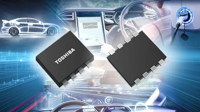
The TPDY110F is designed for automotive use. Image used courtesy of Toshiba
Eliminating the 0.7 Penalty
Silicon diodes and Schottky devices remain the default choice for reverse-current protection and power OR-ing on automotive supply rails. However, their forward voltage becomes a meaningful liability as ECU current consumption increases.
A standard silicon diode conducting 12 A dissipates roughly 8.4 W continuously. This heat must be managed through copper, derating, or heat sinking. A Schottky device reduces that figure to around 3.5 W, but the loss is still substantial in a power budget where every watt of excess dissipation translates to board area and thermal design effort.
The problem is structural and getting worse. Modern ECUs integrating ADAS sensors, connectivity radios, and high-resolution displays draw significantly more current than the older vehicle electronics. Simultaneously, ISO 26262 functional safety requirements are encouraging the use of dual-rail architectures, in which two supply paths feed the same load. Each rail typically uses its own diode, so the voltage drop and power loss occur twice.
An ideal diode controller addresses both pressures by substituting a low-RDS(on) N-channel MOSFET for the diode, at 10 to 15 mΩ, forward drop at 12 A falls below 20 mV, and power loss drops under 0.25 W, more than 30 times lower than a conventional diode.
Key Specifications of the TPD7110F Controller
The TPD7110F supports an input voltage range of 3 V to 32 V. It is housed in Toshiba's PS-8 surface-mount package, measuring 2.9 mm × 2.8 mm, approximately half the mounting area of the MSOP-8 packages used by most competing ideal diode controllers.
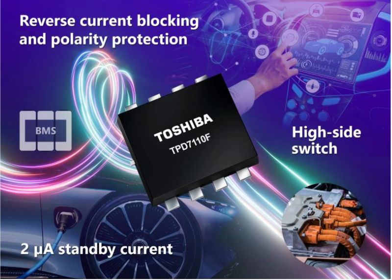
The TPD7110F controller. Image used courtesy of Toshiba
The TPD7110F uses an integrated charge pump with an internal capacitor to drive the gate of an external N-channel MOSFET above its source voltage on the high side of the supply line. Including an internal pump capacitor eliminates the external capacitor that competing solutions require. This reduces component count and supports high-density PCB layouts, all while reducing BOM costs.
The controller continuously monitors the drain-source voltage of the external MOSFET. When VDS goes negative, indicating current is trying to flow from the load back to the battery, the device rapidly pulls the gate low, turning the MOSFET off and interrupting the unwanted current path.
This reverse-current blocking is particularly significant in redundant power-supply rail designs, where two sources feed the same load through parallel paths. A diode isolates each rail passively but burns its forward drop on every cycle. The TPD7110F isolates actively and at near-zero forward loss, keeping both rails at full efficiency.
Notably, the reverse current-blocking function can be disabled, which gives the TPD7110F its versatility across different power management configurations.
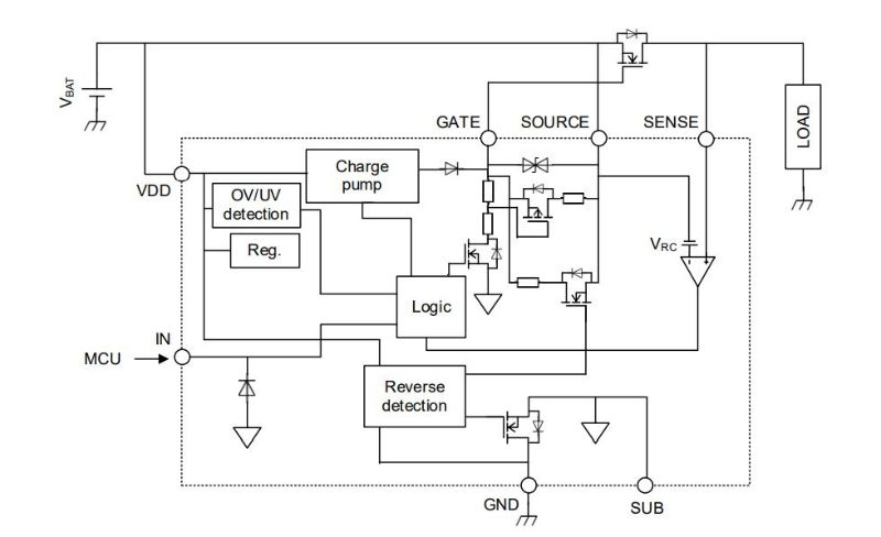
Block diagram of the high-side N-channel MOSFET gate driver. Image used courtesy of Toshiba
In a BMS design where the battery must occasionally charge through the same power path the device is protecting, bidirectional current flow is a requirement, not a fault condition. Disabling reverse current blocking converts the TPD7110F from a unidirectional ideal diode controller into a low-loss high-side switch that passes current in both directions, without changing the IC or the surrounding circuit topology.
Additionally, combining it with a back-to-back MOSFET configuration, where two FETs are connected source-to-source and both driven by the controller, the device can also act as a fully commanded ON/OFF load switch.
These three operating modes: ideal diode, bidirectional switch, and load switch, are available from the same package, making the TPD7110F applicable across BCM power entry stages, BMS isolation circuits, and other automotive power nodes.
The controller draws just 100 μA when the output is on, reducing to 2 μA in standby mode, and handles the full automotive temperature range of -40 to 125 °C.
More information can be found in the datasheet.
Looking Ahead
As automotive E/E architectures shift toward zonal designs, the number of rail isolation and protection points per vehicle grows substantially, and each one is a candidate for a discrete diode that could instead be an integrated ideal diode controller. Toshiba's integration of the charge pump capacitor is a specific response to the cost and space pressures that make discrete solutions less attractive at scale.
As ECU current budgets continue to rise and redundant power rail requirements become more common across more vehicle classes, the efficiency gap between a conventional diode and an ideal diode controller will only widen.