Facebook
 Google
 GitHub
 Linkedin
A Blueprint for EV Power Converters
As the era of the internal combustion engine fades and electric motors pick up steam, the auto industry looks to the semiconductor industry for the electronics innovations needed to deliver an electrified future.
This article is published by EEPower as part of an exclusive digital content partnership with Bodo’s Power Systems.
As the era of the internal combustion engine as the vehicle’s primary power source fades, it is the electric motor the automotive industry favors as the alternative. In turn, automotive OEMs look to the semiconductor industry for the electronics innovations needed to deliver this electrified future. Battery electric vehicles (BEV) are the preferred approach, and everyone is looking to lead in the knowledge necessary to make them as appealing as possible. However, many get overexcited about the gadgets and features inside the car, and vehicle range and charging remain key concerns.
Wide bandgap (WBG) technologies, such as Silicon Carbide (SiC), benefit from this change of power source in automotive and offer substantial advantages over traditional power devices, such as IGBTs, that we’ve previously relied on. The passive component manufacturers are working hard, too. Innovation in inductors helps to ensure the benefits of WBG as a faster switching topology to deliver more range and faster, more reliable charging technology.
All of this is backed by tangible demand. Revenue from electric vehicles is expected to reach over $620 billion in 2024 and grow at 10% per year, which will see more than 13 million BEVs added to roads by the end of the decade. With new generations of SiC MOSFETs being released and improved passives regularly being rolled out, most engineers will wonder how to evaluate their benefits effectively and efficiently.
Commonalities in EV Power Converter Blocks
One area of focus is EV charging. Both BEVs and plug-in hybrids (PHEV) have an onboard charger (OBC) supporting power ranges of 3.6 kW to 22 kW. These can be supplied with AC through a dedicated wall box or charging station at home, on the roadside or in a car park. For vehicles parked at home or work, it’s ideal for topping up while the car rests. When it comes to longer journeys, DC chargers provide fast charging en route. Delivering 40 – 300 kW or even more, these bypass the OBC to deliver an 80% charge in around 20 to 60 minutes.
The basic structure of the charger is the same in both cases. AC is fed into a power factor correction (PFC) unit, followed by a DC/ DC converter that supplies the vehicle battery’s charging circuitry (Figure 1).
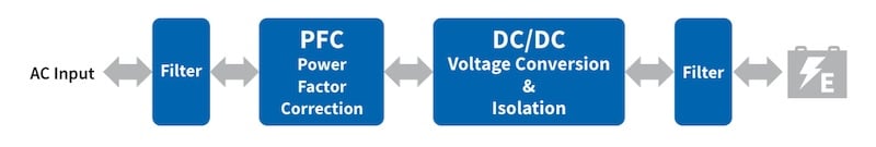
Figure 1. Basic blocks of an EV charging system. Image used courtesy of Bodo’s Power Systems [PDF]
Power efficiency is vital to minimize heat dissipation and save energy, while available space and design weight targets place pressure on power density requirements. Furthermore, EVs are seen as a potential power source to balance out electrical grid disturbances (vehicle to grid, V2G) or even provide power to homes in emergencies (vehicle to home, V2H). Chargers need bidirectional topologies, leading us toward totem pole-style PFCs, dual-active bridge (DAB), and LLC DC/DC converters. All these topologies make use of a bridge leg, and, looking at a motor inverter of an EV, this electronic element appears there, too.
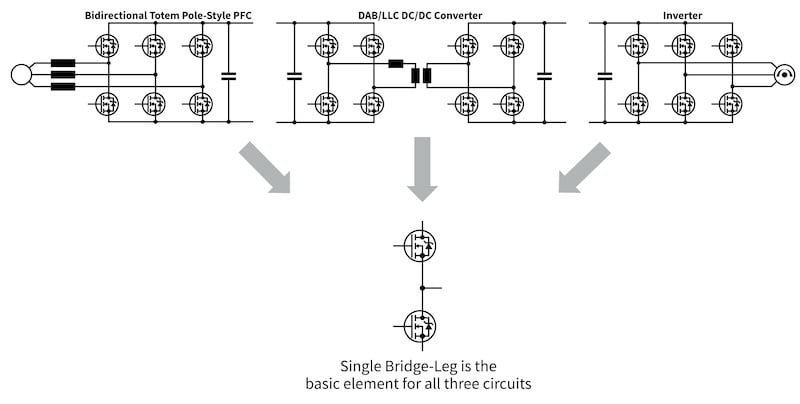
Figure 2. A bridge-leg is common in PFC, DC/DC, and inverter designs. Image used courtesy of Bodo’s Power Systems [PDF]
Modular Approach to Exploring SiC-Based Designs
None of the topologies discussed are simple to design, with high voltages and currents at play during testing. However, the repeated circuit elements within these topologies offer a chance to use modularity to rapidly evaluate different approaches. For example, the input inductors, single bridge legs, and the output capacitor can be isolated within the circuit of a PFC. Input and output voltage and current measurement, along with control of the SiC MOSFETs, can then be assigned to a fourth element performing system control. For this purpose, a microcontroller dedicated to digital power converter applications is ideal (Figure 3).
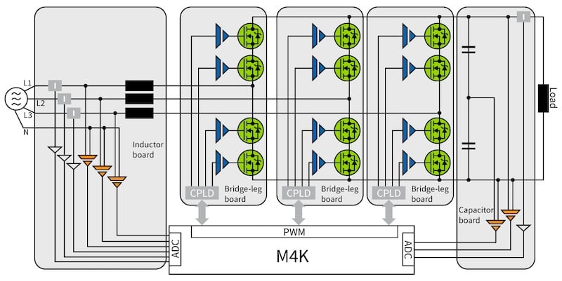
Figure 3. The PFC can be broken down into an input inductor, an output capacitor, a bridge-leg, and a control block. Many blocks are also used in DC/DC converters and motor inverters. Image used courtesy of Bodo’s Power Systems [PDF]
This is the approach used to develop the feasibility study for the Modular EV Charger Reference Design Concept (Figure 4) that Toshiba has been undertaking to explore creating a compact design while meeting the power level requirements. It breaks the design down into seven printed circuit boards (PCB). At its core are the switching boards featuring four SiC MOSFETs in a three-level neutral point clamped (NPC) design. This supports sharing thermal load and voltage stresses across the switches and reduces volt-second ripple on the inductors. Two SiC Schottky barrier diodes (SBD), four gate drivers, and a complex programmable logic device (CPLD) to generate precise switching and the required four control signals round out the design.
The SiC MOSFETs include an on-die integrated built-in Schottky Barrier Diode (SBD) with a forward voltage of just 1.35V. This integrated SBD is key to limiting on-resistance changes over the operational lifetime. RDS(ON) × Qgd (gate-drain charge) is also 80% lower than second-generation SiC devices, while the wider VGSS rating of -10V to +25V simplifies gate driver circuit design.
Like in any power converter, optimal control of the switches over the application’s lifetime is required. This is implemented using an optically isolated TLP5214 gate driver that delivers a ±4.0A output for fast switching, which is then paired with Toshiba’s third-generation SiC MOSFETs. The driver also features an integrated active Miller clamp to avoid parasitic dV/dt-triggered turn-on.
Leveraging Features for a Compact Cube PFC Design
To achieve a compact cube design at the power levels demanded, interconnects are implemented in the high current paths using copper rails and the mechanical metal spacers that hold the boards together. This leads to an increase in the implementation’s parasitic inductances, limiting the switching speeds that can be used but keeping the PCB technology simple.
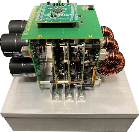
Image used courtesy of Bodo’s Power Systems [PDF]
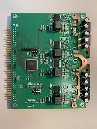
Figure 4. Details of the current-carrying mechanical interconnects and copper rails in the SiC Cube PFC design. Image used courtesy of Bodo’s Power Systems [PDF]
The inductor and capacitor boards (Figure 5) both feature the same current and voltage measurement circuitry. Current is measured using Hall sensors, while voltage is measured differentially using a TLP7820 isolated operational amplifier. On its input side, these use a sigma-delta analog-to-digital (ADC) converter to drive an LED. The resultant optical signal feeds into an amplifier converted through a 1-bit digital-to-analog converter (DAC) and low-pass filter. This approach offers high gain accuracy (±0.5%), small gain drift (0.00012 V/°C), and low non-linearity (0.02% for VIN = ±200 mV). TLP7820 is UL/cUL recognized, and VDE/CQC approved.
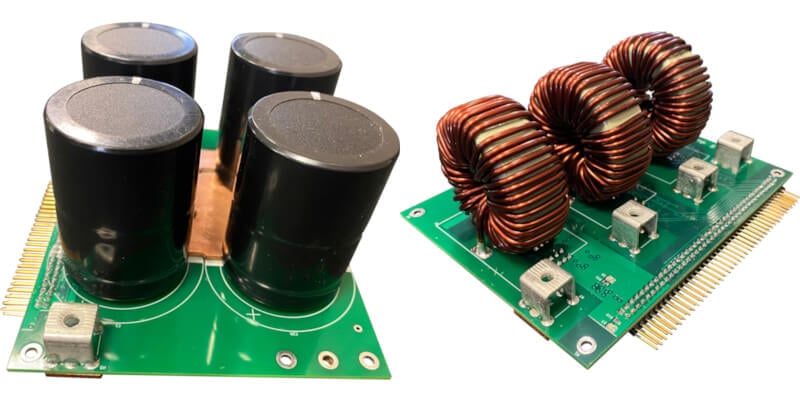
Figure 5. Both the capacitor and inductor boards feature the same current and voltage-measurement circuitry. Image used courtesy of Bodo’s Power Systems [PDF]
Traversing the bridge-leg, capacitor, and inductor boards is the controller board featuring a TXZ+ Arm Cortex-M4F microcontroller. What makes it particularly suited to digital power control is its advanced pulse-width modulation (PWM) modules that include a three-phase complementary output with dead-time control. Furthermore, it can be synchronized in hardware with analog measurements made by the 12-bit on-chip ADCs. Three gain-selectable operational amplifiers are also available. The microcontroller also features a Vector Engine block that can offload and accelerate complex calculations like sin and cos and Clarke and Park transformations, which is also beneficial for PFC and motor inverter applications.
High Power Density With Reusability
Leveraging the latest SiC MOSFET technology, this compact cuboid PFC design targets to deliver 22 kW at a power factor of 0.99 and an efficiency of up to 99%. Measuring 140 × 140 × 210 mm3, that translates to a power density of 3 kW/dm3. Thanks to its modularity, the bridge-leg SiC MOSFET, capacitor, inductor, and microcontroller boards can easily be trialed in other power converter applications, thus easing the development burden. By creating this modular design concept, Toshiba aims to support development teams new to WBG technology and enable the exploration of the robustness, lower RDS(ON) over operational temperature, and higher switching frequency capabilities of SiC MOSFETs, which are still, for many, a new technology.
Next Steps: Further Evaluation and Development
Toshiba strives to offer comprehensive support to engineers and development teams venturing into the realm of SiC-based design. Typically, this support encompasses detailed documentation that covers every aspect of the reference design, including technical specifications, application notes, and design guidelines to facilitate a smoother development process.
The SiC Cube concept was initially presented at Bodo’s Wide Bandgap event in Munich at the end of 2023. Presently, the SiC Cube feasibility study is assessing whether the modular and multi-level approach works effectively. Currently, application support is available, with the schematics, board data, and BOM information for SiC Cube being established. Additional documents and resources will be available in the future.
This article originally appeared in Bodo’s Power Systems [PDF] magazine.