 Facebook
 Google
 GitHub
 Linkedin
Understanding Linear MOSFETs and Their Applications
Linear-mode applications such as class-A audio amplifiers, active DC-link discharge, battery charge-discharge, inrush current limiter, low-voltage DC motor control, or electronic loads demand the power MOSFETs to be operated within the current saturation region. Standard MOSFETs are prone to ETI when used in linear-mode applications leading to possible device destruction. Linear MOSFETs are the most appropriate choice for linear-mode applications to ensure reliable operation.
Introduction – What is linear-mode operation and why is it required
Power MOSFET’s output characteristic can be divided in to three distinct regions namely ohmic region, non-linear region, and saturation or active region as displayed in Figure 1. In the ohmic region, the drain current ID is directly proportional to the drain-source voltage VDS for a given gate-source voltage VGS. The MOSFET acts as a resistor in this operation mode with a value equal to its on-state resistance RDS(ON). In the non-linear region, the MOSFET’s resistance behaves non-linearly and the rate of increase of ID with VDS slows down. In the active region, the MOSFET’s channel is saturated with majority charge carriers. In this region, ID is independent of VDS. ID is governed only by VGS and it remains constant for any given VDS. In other words, the MOSFET exhibits the behavior of a constant current sink. This operating mode is commonly known as linear operation mode of power MOSFETs. In this operating mode, the MOSFETs typically dissipate higher power levels than they would in the more common switched-mode applications due to simultaneous occurrence of high voltage and current[1].

Figure 1. Power MOSFET Output Characteristics. Image used courtesy of Bodo’s Power Systems
Why standard MOSFETs are not suitable for linear-mode operation
In practice, the junction temperature Tvj is not uniform across the power MOSFET die. Typically, the temperature at the edge of the MOSFET die, where it is soldered to the mounting tab of a power package, is lower than in the center of the die. This is the result of lateral heat flow. Die temperature variations are mostly harmless in switched-mode operation. However, these variations can trigger catastrophic failure in linear-mode operation. Large power dissipation PD in linear-mode gives rise to electro-thermal instability (ETI) when the rate of power generation is higher than the rate of power dissipation. ETI can be understood as the result of a positive-feedback destruction mechanism on the surface of a power MOSFET forced into linear-mode of operation:
1. There is a local increase in junction temperature Tvj
2. Increasing chip temperature causes local decrease in the gate threshold voltage VGSTH because of its negative temperature coefficient
3. Decreasing threshold voltage causes an increase in local current density JDS such that
4. The increase in current density causes an increase in local power dissipation, which leads to a further local increase in junction temperature
As depicted in Figure 2, the MOSFET equivalent circuit contains the parasitic NPN-transistor which is inherently formed by the sequence of n- and p-doped areas. Depending on the duration of the power pulse, heat transfer conditions, and design of the MOSFET’s cells, ETI may cause a concentration of all drain-current into a current filament and formation of a hot spot. This normally causes MOSFET cells in the affected areas to lose gate control and turns on the parasitic transistor with subsequent destruction of the device [2].

Figure 2. MOSFET Equivalent Circuit. Image used courtesy of Bodo’s Power Systems
Littelfuse Offering in Linear MOSFETs
In response to the problems caused by ETI, Littelfuse has developed a range of power MOSFET structures and processes that provide an extended Forward Bias Safe Operating Area (FBSOA) by eliminating the positive feedback loop. These devices are known as Linear MOSFETs L and L2 family within Littelfuse’s MOSFET product portfolio [5]. The design of these Linear MOSFETs features a nonuniform distribution of transistor cells, as well as cells with different threshold voltages [3]. Every transistor cell is designed with a ballast resistor at its source to limit its current. The parasitic transistor of each cell is heavily bypassed so that it will not turn on even under extreme electrical stress conditions. The linear MOSFETs designed in this way achieve an extended FBSOA capability by suppressing the positive feedback that leads to electro-thermal instability [4]. Linear MOSFETs from Littelfuse are available in wide voltage and current ranges in numerous discrete packages as displayed in Table 1. The MOSFET families Linear L and Linear L2 differ primarily in terms of operating voltage and channel resistance RDS(ON). There are no special gate drive requirements for linear MOSFETs. The IXYS gate driver family IXD_604 can be used for this purpose which is available in a standard 8-pin DIP, 8-pin SOIC, 8-pin Power SOIC with an exposed metal back and an 8-pin DFN (D2) package.

Table 1. Littelfuse Linear MOSFET Portfolio
FBSOA comparison: Standard vs. Linear MOSFET
The Forward Bias Safe Operating Area (FBSOA) is a datasheet Figure of Merit (FOM) that defines the maximum allowed operating points. It is important for the safe operation of MOSFETs to operate within limits of the FBSOA. The typical FBSOA characteristic is bound by the RDS(ON) limit line, current limit line, power limit line, and voltage limit line as represented in Figure 3. By comparing the datasheets of a standard MOSFET and a linear MOSFET, it is evident that the linear MOSFET exhibits the extended FBSOA which means its maximum power handling points for any given pulse width are shifted towards the voltage limit line as illustrated in Figure 3. The typical nature of linear-mode operation demands high power dissipation in the device. By comparing both the FBSOAs it is evident that linear MOSFETs can handle 24%, 31%, 48%, 73% and 118% higher power compared to standard MOSFET for 25µs, 100µs, 1ms, 10ms pulse width and continuous operation (DC) respectively. Therefore, the linear MOSFETs are more suitable devices for linear mode applications than standard MOSFETs.

Figure 3. Datasheet FBSOA Comparison: Standard MOSFET IXTH30N60P vs. Linear MOSFET IXTH30N60L2. Image used courtesy of Bodo’s Power Systems
FBSOA comparison: Littelfuse Linear MOSFET vs. Competition’s MOSFET
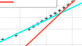
In the linear-mode applications, MOSFETs are usually operated at low frequencies with long pulse widths of 10ms or more. The linear MOSFET IXTH2N150L, a 1500V 2A TO-247 packaged device, which is one of the most popular devices in electronic load applications, was tested and compared in the lab to the nearest competition device, a 1500V 2.5A TO-247 packaged component. The FBSOA measurement set-up consists of an apparatus which generates a power pulse for measurements, the Device Under Test (DUT) mounted on a copper heat-sink, and a thermo couple for case temperature TC measurement as depicted in Figure 4a. The Maximum power which the device can withstand was measured for different pulse widths on both DUTs. Figure 4b shows the quantitative comparison between both device in terms of maximum power withstand capability using various pulse widths. It can be observed that the Littelfuse device is able to handle significantly higher power than the competing device, especially for long pulse widths ≥10ms and continuous operation. Such robust performance translates into the improvement of overall system reliability in linear-mode applications.

Figure 4a. Datasheet FBSOA Comparison: Standard MOSFET IXTH30N60P vs. Linear MOSFET IXTH30N60L2. Image used courtesy of Bodo’s Power Systems

Figure 4b. FBSOA Comparison: Competition vs. Littelfuse Linear MOSFET. Image used courtesy of Bodo’s Power Systems
Application Example: Electronic Load
An electronic load is a test instrument which sinks current. It is commonly used to test power sources such as DC-DC converters, fuel-cells, batteries, solar panels, or power supplies under various loading conditions. Figure 5 represents the simplified schematic of an electronic load. The DUT is loaded with the desired current via the control voltage Vcontrol set point. The linear MOSFETs (S1, S2, … , Sn) act as a variable resistor which regulate the current through the load. The MOSFETs are usually arranged in parallel to cater higher power. Apart from linear MOSFETs and gate drivers, Littelfuse offers also offers additional components that are commonly found in electronic loads. Diagramed in figure-5, fast acting fuses (F1, F2,…, Fn), unidirectional and bidirectional transient voltage suppressors (TVS, TVS1, TVS2,…, TVSn), and NTCs for semiconductor temperature monitoring (NTC1, NTC2,…, NTCn) are all products within the Littelfuse portfolio [5].

Figure 5. Simplified Schematic of an electronic load based on linear MOSFETs. Image used courtesy of Bodo’s Power Systems
Conclusion
Linear-mode applications demand the power MOSFETs to be operated within the current saturation region. Standard MOSFETs are prone to ETI when used in linear-mode applications leading to possible device destruction. Linear MOSFETs are the most appropriate solution for linear-mode applications to ensure reliable operation. The FBSOA comparison between a Littelfuse linear MOSFET and the nearest competition reveals the superior power handling capability of the Littelfuse device. The reasons why Littelfuse linear MOSFETs are the most preferred choice is because all the linear devices are 100% tested to guarantee FBSOA, long term availability of parts and high-power dissipation capability thanks to its low thermal resistance junction-to-case RthJC. Littelfuse is the most reliable partner, offering major components such as linear MOSFETs, gate drivers, high-speed fuses, TVS diodes and temperature sensing solutions in the entire value chain of linear-mode applications.
References
[1] Baliga, B. Jayant, ‘Fundamentals of Power Semiconductor Devices’, Springer, 2008.
[2] White Paper: 'MOSFETs Withstand Stress of Linear-Mode Operation', https://www.littelfuse.com/products/power-semiconductors/discrete-mosfets/n-channel-linear.aspx.
[3] Zommer, Tsukanov, 'Non-Uniform Power Semiconductor and Method for Making Non-Uniform Power Semiconductor', U.S. Patent No. US 7157338 B2, Jan 2007.
[4] Zommer, Tsukanov, ‘Non-Uniform Power Semiconductor Device’, U.S. Patent No. US 6710405 B2, March 2004.
[5] Littelfuse offering on https://www.littelfuse.com/products.aspx.
This article originally appeared in Bodo’s Power Systems magazine.


Hola José. Buen artículo. Gracias.