Facebook
 Google
 GitHub
 Linkedin
Controller HIL Testing for GaN and SiC Converters
The high switching frequencies of converters with GaN and SiC components pose a challenge for real-time simulators used for hardware-in-the-loop testing of control systems.
This article is published by EEPower as part of an exclusive digital content partnership with Bodo’s Power Systems.
When the switching frequency of power semiconductors exceeds 100 kHz, it is not sufficient to reduce the simulation step to just below one microsecond. In addition, the gate signals must be oversampled and averaged over one simulation step. This approach works well on CPU- and FPGA-based simulators for hard-switching inverters in continuous conduction mode. However, it becomes inaccurate for resonant converters or dual active bridges, where the currents frequently change direction or enter discontinuous conduction mode. Very small simulation steps of a few nanoseconds are required to accurately simulate such converter topologies, which can only be realized with special algorithms on an FPGA.
Electrical circuit simulation helps design engineers predict and analyze the behavior of an electrical device or system before a prototype is built. Simulation allows engineers to create a model or virtual prototype for the device and perform tests under normal and faulty operating conditions. Since modifications to the model can be made quickly, simulation accelerates the development process and reduces time-to-market for new products. Simulation is helpful in the early design phase and in testing the correct operation of an existing device that will be part of a larger system.In power electronics, digital real-time simulators are increasingly employed to test and validate control equipment without the actual power circuit being available. The actual power circuit, which represents the controlled system, is replaced by an appropriate dynamic model computed on the simulator. Since the control equipment is embodied as electronic hardware, this use case is called controller hardware-in-the-loop (HIL) testing.
Image used courtesy of Adobe Stock
HIL simulations allow the control hardware and software to be tested in a safe environment. When simulating power electronics in real-time, the small time constants and fast dynamics of the electrical circuit pose challenges. To make the control equipment under test operate like when it is connected to a real power circuit, the real-time simulator must feature high fidelity and low loop-back latency. This means the simulation results must accurately represent the real voltages and currents in the electric circuit, and they need to be computed and output within a few microseconds after a signal has changed at the simulator’s input.
With the advent of wide bandgap devices such as GaN and SiC MOSFETs, the switching frequencies of power converters have advanced into the MHz range. This is a challenge for real-time simulators, as their minimum simulation time step typically lies between 100 ns and a few microseconds. However, to capture a PWM signal with sufficient accuracy, it must be sampled with a rate of at least 100 times the switching frequency. In the case of a switching frequency of 1 MHz, this translates into a sampling interval of 10 ns or less.
Two techniques that facilitate real-time simulations with such small sampling intervals are sub-cycle averaging and Nanostep. While sub-cycle averaging can be applied to a wide class of inverters primarily operating in continuous conduction mode (CCM), a Nanostep solver is perfectly suited for the simulation of high-frequency and resonant DC/DC converter topologies such as the dual-active bridge (DAB) and LLC.
Common power supply architectures combine an AC/DC converter and a high-frequency DC/DC converter. A typical example is an EV charger consisting of a 3-phase active front-end (AFE) and a DAB, as shown in Figure 1. In this 10 kW charger based on wide bandgap technology, the AFE operates in CCM at 140 kHz while the DAB switches at 500 kHz.
With upcoming firmware upgrades for the RT Box 2 and 3, such a charger circuit can be simulated on the FPGA fabric inside the RT Box. The AFE would be simulated with sub-cycle averaging, while the DAB would require a dedicated Nanostep solver. This combination of solver techniques enables highly accurate real-time simulations of power converters with high switching frequencies.

Figure 1. System schematic for EV charger with active front-end (AFE) and dual-active bridge (DAB). Image used courtesy of Bodo’s Power Systems [PDF]
Sub-Cycle Averaging
In power electronic applications, many inverter-converter systems, such as buck converters, boost converters, diode rectifiers, and voltage source inverters (VSIs), can be realized with one or more half-bridges. These half-bridges consist of series-connected power semiconductors, each of which can be naturally commutated devices (e.g., diodes), forced commutated devices (e.g., IGBTs), or a combination of both.
In most applications, the half-bridges are connected to a capacitor or voltage source on the DC side. Under normal operation, it can be assumed that the DC voltage vdc is positively biased, since otherwise, the diodes would short-circuit the DC link. During operation, the phase terminal switches to the positive or negative DC link voltage or remains unconnected.
For sub-cycle averaging, such half-bridges are modeled with a combination of two series-connected diodes and multiple controlled voltage and current sources to increase the fidelity of real-time simulations. This modeling approach is illustrated in Figure 2 for a VSI half-bridge. The voltage sources va1 and va2 are controlled by the switching signals sp and sn. They apply the DC voltage vdc to the phase side. Likewise, the current source idc is controlled by the same switching signals applying the phase current ia1 or ia2 to the DC side.
The two diodes are required to simulate natural commutation and discontinuous conduction mode (DCM). Depending on the direction of the phase current, the lower or upper diode will conduct, which applies the corresponding phase voltage and DC. If none of the diodes conduct, the half-bridge has entered DCM, which means it is zero.
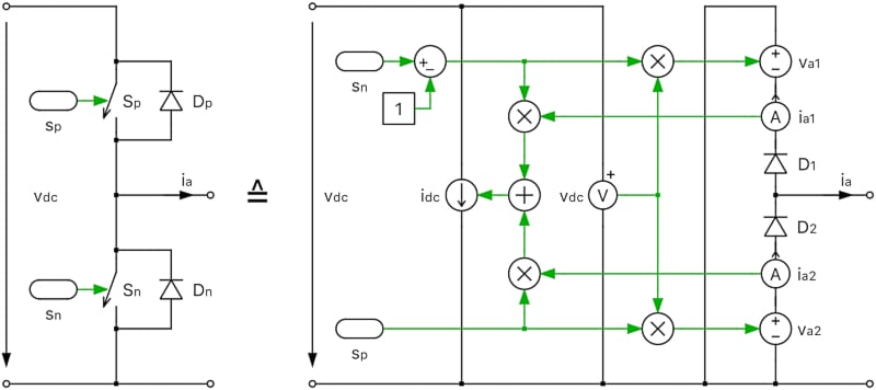
Figure 2. Sub-cycle average model for a VSI half-bridge. Image used courtesy of Bodo’s Power Systems [PDF]
The key advantage of sub-cycle averaging is that the switching signals can not only be binary signals representing the on-state (s = 1) and off-state (s = 0) of the device but can also be short-term average values (0 ≤ s ≤ 1) representing the relative on-time or duty cycle of the device during a simulation step. These average values can be obtained by sampling the PWM signals at each FPGA clock cycle, typically shorter than 10 ns. Even with high switching frequencies and simulation steps two orders of magnitude larger than the FPGA clock cycle, the resulting phase current is essentially accurate because the applied volt-seconds of the average signals correspond to the volt-seconds of the original PWM signals. However, not all switching harmonics can be preserved with large simulation steps. If the step size is too large, the calculated voltages and currents may have a gross error.
The main disadvantage of sub-cycle averaging is the inaccuracy caused by the zero crossing of the phase current. As the direction of the phase current is determined only once per simulation step, slightly incorrect volt-seconds may be applied during the step in which the current has crossed zero or has entered DCM. While this inaccuracy is acceptable for inverters operating in CCM and without frequent changes in the current direction, such as grid-connected VSIs, this may not be the case for other converters, especially naturally commutated converters, operating at high switching frequencies.
Figure 3 depicts the 3-phase AFE circuit from the EV charger example. The AFE with SiC MOSFETs switching at 140 kHz is the benchmark model for validating the sub-cycle averaging technique. In this circuit model, the load of the DAB stage is represented by an equivalent resistor Rout.

Figure 3. AFE circuit with SiC MOSFETs. Image used courtesy of Bodo’s Power Systems [PDF]
Figure 4 shows the input currents of the AFE during a step change from half load to full load. Offline simulations generated the reference results in PLECS with a variable step solver and ideal switches. They are compared with the waveforms obtained from real-time simulations with the RT Box. The model step of 400 ns corresponds to the step size that can be achieved on an RT Box 2 or 3 by using the new FPGA-based circuit solver with sub-cycle averaging. The control signals for the MOSFETs are generated by an open-loop controller to allow a direct comparison between the two different modeling approaches.
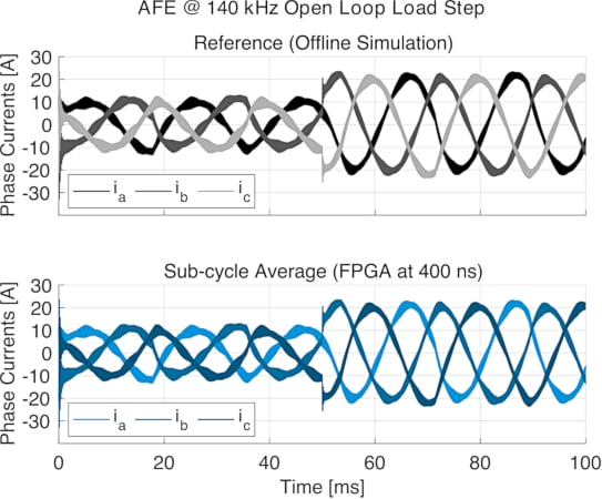
Figure 4. Offline simulation with PLECS compared to real-time simulation on the RT Box. Image used courtesy of Bodo’s Power Systems [PDF]
The comparison of the phase currents demonstrates the accuracy of the sub-cycle average model. Figure 5 shows the AC in phase A for a single cycle of the line frequency. The FPGA-based simulation at 400 ns closely matches the reference waveform. However, the sub-cycle average approach requires a small model step size for an accurate solution. At a step size of 2 μs, which is representative of computing the sub-cycle average model on a CPU core of the RT Box, the current waveforms exhibit a large error.
This error is caused by the delayed detection of changes in the current direction, which can occur when the PWM pulses are shorter than the step size of the simulation. In the model in Figure 2, the peak values of the averaged voltages va1 and va2 may not be large enough to make the phase current commutate directly from one diode (D1 and D2) to the other. Instead, both diodes may open and clamp the current to zero. This effect can be observed in Figure 5, where at a step size of 2 μs, the phase A current is distorted around the zero crossings. The same behavior in phases B and C manifests itself in distortions near the peak of the phase A waveform via a shift in the neutral voltage.
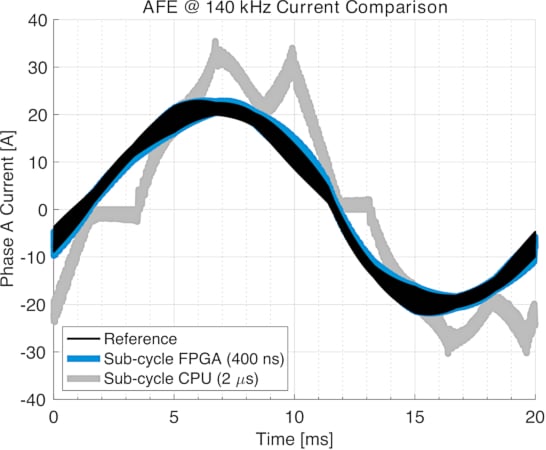
Figure 5. Phase A current waveform over one line cycle. Image used courtesy of Bodo’s Power Systems [PDF]
Figure 6 illustrates in detail how the direction of the phase current changes from negative to positive. Despite the repeated zero-crossings, the FPGA-based simulation deviates slightly from the reference. With the 400 ns step size, the solver executes nearly 18 times within a switching cycle, so the averaged voltage values are often close to the instantaneous voltages. Occasional clamping of the current to zero, caused by open diodes, is transitional and has only a minor impact on the results. On the contrary, if the voltages are averaged over a CPU model step of 2 μs, they fail to commutate the current.
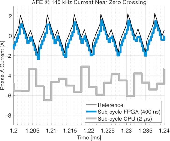
Figure 6. Detailed view of phase A current waveform. Image used courtesy of Bodo’s Power Systems [PDF]
Nanostep
The sub-cycle average approach becomes inaccurate for power electronic converters where the direction of the phase current changes frequently. This is especially true for DC/DC converters with an inductive AC link, where the power transfer is very sensitive to the phase shift between the current and the PWM signals. A delayed zero-crossing detection of the AC can lead to considerable errors. This is because positive, negative, and zero currents correspond to a different circuit topology governed by another set of differential equations.
To detect zero crossings as fast as possible, Plexim has developed the Nanostep solver that will be available for the RT Box later this year. In a Nanostep simulation, the values for the inductor currents and the voltages of the resonant capacitors are updated with each FPGA clock cycle. Since calculating a new value requires a pipeline of arithmetic operations and takes multiple clock cycles, the values for all possible topologies are computed in parallel. The validity of a topology depends on the most recent gate signals and the latest direction of the inductor current. An inductor current that changes direction or is clamped to zero represents a boundary condition that limits the validity range of certain topologies. The decision on which topology must be applied is only made after all values have been calculated and is based on the boundary conditions.
Figure 7 shows a nanostep model of the EV charger’s DAB stage. The converter switching frequency is 500 kHz, and the dead time is 120 ns. A phase shift between the primary and secondary switch modulation controls the power transfer.
The Nanostep solver incorporates the converter’s switching network and energy storage elements. Gate signal sampling, inductor current integration, and current zero-crossing detection occur at the FPGA clock cycle of 5 nanoseconds or less. With a 5 ns sample rate, the Nanostep solver can detect phase shifts as low as 0.5 % for a 500 kHz switching frequency.

Figure 7. Nanostep model for a dual active bridge interfacing with an external circuit. Image used courtesy of Bodo’s Power Systems [PDF]
The external circuit dynamics of interest, namely the input and output capacitor voltages vHV and vLV, are usually significantly slower than the dynamics of the internal switching network. The external circuit is simulated using a generic solver implemented on the FPGA or CPU with a much larger model step. Typical step sizes range from a few hundred nanoseconds to a few microseconds. In this application, the 400 ns model step of the AFE is used as the communication interval with the Nanostep solver. The inputs to the Nanostep solver are the terminal voltages of the converter, sampled at the model step. The Nanostep solver averages the converter’s input and output currents over one model step to correctly calculate the currents iHV and iLV injected into the external network.
The limitations of the Nanostep solver are due to the interface with the external circuit that is solved at a larger model step. The voltages at the converter terminals are assumed constant over a model step. The model step also dictates the update rate of the analog hardware output, affecting the loop-back latency. Lastly, internal fault conditions are not simulated but can be detected when any gate signals within the 5 ns sampling interval would result in shorting the DC terminals of the converter.
Figure 8 benchmarks the accuracy of the Nanostep solver against offline PLECS simulations with ideal switches and a hypothetical sub-cycle average model with a 50 ns step size. The 50 ns model cannot be realized on the RT Box. The converter operates with a constant phase shift of 0.1Tsw or 200 ns. With the larger step size, averaging the gate signals over the 50 ns interval leads to an error in the output current. The zero crossings of the current during the dead time interval are also missed. Comparing the average current over a model step, the Nanostep solver and reference solution are accurate to within 1%, while the model with a 50 ns step size has an error of 40 %.

Figure 8. The output current of DAB was simulated using a 5 ns and 50 ns step size. Image used courtesy of Bodo’s Power Systems [PDF]
Using the average values of the 5 ns Nanostep solver calculations as the interface to the external circuit retains the large-signal dynamics of the converter’s input and output ports. Figure 9 shows the model response for a step change in the modulator phase with a constant resistive load. The converter starts at 500 V output at rated power, steps to a lower power level due to a decrease in phase shift, and then returns to the initial phase. The voltage dynamics of the Nanostep solver, in combination with a 400 ns model step, closely match the reference solution. The additional phase lag is due to the current averaging of the Nanostep solver and the model step duration. The sub-cycle average model is not usable as it delivers excess power, and the output voltage, therefore, never reaches the expected steady-state output voltage.
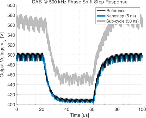
Figure 9. 500 kHz DAB response to a step change in modulator phase shift. Image used courtesy of Bodo’s Power Systems [PDF]
Real-Time Simulation
Real-time simulation can test and validate the control equipment, even for next-generation power converters based on SiC and GaN. Due to the high switching frequencies and short time constants of converters with wide bandgap devices, real-time simulators must capture the gate drive signals with sampling intervals of a few nanoseconds and use special numerical techniques to detect current zero crossings with high time accuracy.
Plexim has developed powerful algorithms to meet these requirements: Sub-cycle averaging is a versatile method for simulating voltage source inverters operating mainly in CCM. In addition, the new Nanostep solver enables real-time simulation of high-frequency and resonant DC/DC converters operating well above 100 kHz. The Nanostep solver detects changes in the current direction with a resolution of 5 ns, making it perfect for selected topologies where the current frequently changes direction or enters DCM.
Firmware upgrades free of charge, to be released in 2024, will enable the RT Box 2 and 3 to simulate sub-cycle average and Nanostep models on the integrated FPGA. Benchmark simulations of a 3-phase AFE at 140 kHz and a DAB at 500 kHz show that these real-time simulation techniques produce highly accurate results.
This article originally appeared in Bodo’s Power Systems [PDF] magazine.