Facebook
 Google
 GitHub
 Linkedin
Toshiba Rolls Out 650 V 3rd Gen SiC MOSFETs
The MOSFETs feature numerous structural and material innovations in a DFN 8x8 package.
Toshiba released its third-generation silicon-carbide (SiC) MOSFETs for industrial equipment, including power supplies in servers and data centers, electric vehicle charging stations, uninterruptible power supplies, and photovoltaic inverters.
Toshiba claims the new family, which boasts a DFN 8x8 package and a suite of architectural and structural enhancements, outperforms competitors and previous generation devices by significant margins.

650 V SiC MOSFETs. Image used courtesy of Toshiba
The 3rd Gen SiC MOSFETs
Toshiba’s third-generation SiC MOSFET introduces a significant advancement in power device architecture through structural and material innovations. The device integrates a Schottky barrier diode (SBD) in parallel with the intrinsic PN body diode to suppress forward voltage drop and to enhance reverse conduction efficiency. This structural approach also prevents crystal defect propagation, which reduces long-term RDS(ON) drift to 3%, compared to 42% observed in conventional non-integrated designs during high-current stress testing.
The MOSFET also leverages nitrogen injection under the p-well and into the JFET region to reduce Rspread and feedback capacitance, which lowers conduction and switching losses without compromising area-specific on-resistance (RonA). At 1200 V ratings, Toshiba reports a 43% reduction in RonA and an 80% reduction in the Ron*Qgd figure of merit versus its 2G counterpart. These enhancements improve efficiency in high-frequency hard-switching applications.
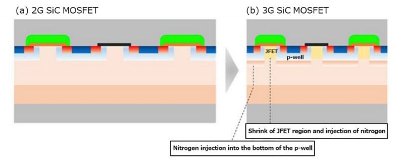
Structure of Toshiba’s 2G and 3G SiC MOSFETs. Image used courtesy of Toshiba
A wide gate voltage range from -10 V to +25 V and a threshold voltage between 3 V and 5 V improve noise immunity and simplify gate driver design. This higher Vth suppresses spurious turn-on during transient conditions, supporting more stable switching behavior in noisy power environments. For example, Toshiba’s TW048N65C device demonstrates RDS(ON) thermal stability, with only a 17% increase at 175°C compared to 25°C. Toshiba claims that this metric outperforms competitors, whose devices show increases of 43% or more.
Meanwhile, efficiency testing in a totem-pole power factor correction (PFC) circuit confirms superior performance under heavy load conditions. With high switching frequency legs populated by the TW048N65C, Toshiba’s device maintained higher conversion efficiency at 1.8 kW load compared to competitor solutions, driven by lower switching losses and reduced dead-time loss through its low VF.
Body Diode Behavior in Hard-Switching Applications
In hard-switching applications such as totem-pole PFC circuits, the behavior of the MOSFET body diode directly impacts both switching efficiency and device longevity.
Traditional silicon MOSFETs rely on intrinsic PN junctions for reverse conduction during dead times, but these diodes exhibit high reverse recovery charge (Qrr), which introduces significant switching losses and generates unwanted EMI. In contrast, SiC MOSFETs have inherently faster reverse recovery characteristics, yet their PN body diodes still exhibit limitations under high current stress. The abrupt turn-off of these diodes during transition periods causes transient voltage overshoot and oscillations, degrading both efficiency and device reliability.
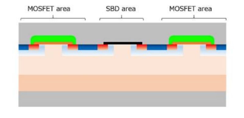
Toshiba device cross-sectional structure with a built-in SBD. Image used courtesy of Toshiba
Modern SiC MOSFET designs integrate an SBD in parallel with the PN body diode. The SBD conducts during reverse current flow, suppressing PN junction activation and virtually eliminating reverse recovery charge. This reduces switching loss and improves waveform integrity during dead time conduction. However, improper SBD design may introduce increased leakage or forward voltage drop, affecting conduction efficiency.
Toshiba’s third-generation SiC MOSFET mitigates these trade-offs through optimized SBD integration. The device suppresses crystal defect propagation by preventing sustained conduction through the PN body diode, thereby limiting long-term RDS(on) drift. The design also reduces the source-to-drain VF across the entire reverse conduction region, lowering conduction loss during synchronous rectification dead time.
MOSFET Efficiency at Scale
Toshiba’s third-generation SiC MOSFETs deliver several impressive performance improvements by refining internal structure and behavior at the device level. Ultimately, using integrated SBDs, enhanced by low-RDS(on) stability and controlled VF behavior, opens the door to more robust designs in multi-kilowatt systems without the penalty of added complexity.