Facebook
 Google
 GitHub
 Linkedin
Addressing SiC MOSFET Packaging Complexities
The growing prevalence of wide bandgap devices requires innovative advancements in packaging technology to fully harness the advantages of WBG semiconductors.
This article is published by EEPower as part of an exclusive digital content partnership with Bodo’s Power Systems.
Isolation of conventional discrete SiC MOSFETs from heatsinks relies on an external, thermally conductive, electrically isolating material. This not only increases thermal resistance junction-to-heatsink but complicates thermal management and creates obstacles in automated and manual assembly processes. Further, poor thermal conductivity reduces power and current handling capabilities, significantly limiting optimal SiC chip utilization.
ISO247 – High-Performance Ceramic-based Discrete Isolated Package
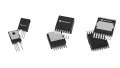
The ISO247 package from Littelfuse, featuring high-performance silicon nitride (Si3N4) ceramic, addresses these challenges, improving SiC chip utilization and enhancing SiC MOSFET-based applications. The ISO247 belongs to the ISOPLUS family of internally isolated discrete power semiconductor device packages and features direct copper bonding (DCB) substrates with aluminum oxide (Al2O3) ceramic, first pioneered by IXYS Semiconductor (now part of Littelfuse) in 2003. The ISO247 adheres to JEDEC TO-247AD, ensuring pin compatibility with the standard TO-247 package. The ISO247 spans a variety of semiconductor technologies, including Si/SiC MOSFETs, IGBTs, and diodes, with voltage classes ranging from 70 V to 1600 V. The ISO247 package, with advanced high-performance silicon nitride ceramic, is specifically tailored to meet the demanding requirements of SiC MOSFET-based applications. It offers the following key advantages compared to standard TO-247:
- High-performance ceramic-based active metal brazing (AMB) substrate offers inherent isolation, higher thermal conductivity, and reduced thermal resistance junction-to-heatsink
- Isolation voltage rating of 2.5 kV AC, 1 minute or 3 kV AC, 1 second
- Higher temperature and power cycling in seconds (PCsec) withstand capability ascribed to the matched coefficient of thermal expansion (CTE) for SiC chip and AMB substrate
- Increased power density and simplified thermal management
- Reduced electromechanical interference attributed to the small chip-to-heatsink stray capacitance
Image used courtesy of Adobe Stock
Although ISO247 and TO247 packages share identical outer dimensions and pinout configurations, their internal structures and mounting approach exhibit notable distinctions as depicted in Figure 1. While the TO-247 device necessitates external isolation during its attachment to the heatsink, the ISO247 device employs only thermal interface material for its mounting to the heatsink. Note: The thermal interface material provides no electrical isolation, its function is only to improve thermal conductivity.
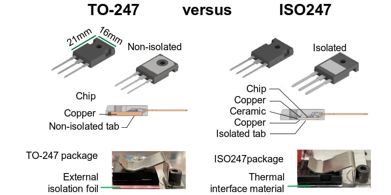
Figure 1. Internal construction and mounting difference between TO-247 vs. ISO247 packages. Image used courtesy of Bodo’s Power Systems [PDF]
Thermal Performance Comparison: ISO247 and TO-247
The standard TO-247 package has an electrically conductive mounting tab, which is typically at the drain potential. It is generally desirable to electrically isolate the device mounting tab from the heat sink due to safety concerns and the desire to mount multiple discrete devices on the same heat sink frame. The utilization of an external, thermally conductive, electrically isolating foil between the semiconductor package and the heatsink has become a widely adopted approach in the industry for this purpose. Nonetheless, employing external isolation entails significant drawbacks. Increased thermal resistance, diminished power and current handling capacity, complex thermal management, and substantial assembly efforts are each either direct or indirect consequences of external isolation tactics. The mentioned penalties, particularly the issue of reduced power handling capabilities, become unacceptable, especially in cases where wide-bandgap (WBG) semiconductors like SiC MOSFETs are utilized.
To evaluate the performance advantages of the advanced ISO247 package, thermal measurements were conducted using a 1200 V, 25 mΩ SiC MOSFET chip in various packaging and thermal interface configurations summarized in Table 1. Thermal measurements were executed using the cooling curve method in accordance with IEC 60747-8, with measurement set-up detailed in reference.
Table 1. ISO247 and TO-247 devices for thermal performance comparison featuring SiC MOSFETs.
|
Device |
Device 1 |
Device 2 |
Device 3 |
|
Chip |
1200 V, 25 mΩ SiC MOSFET |
||
|
Package |
TO-247 |
TO-247 |
ISO247 |
|
Device-to-eatsink Isolation |
External isolation foil with thermal conductivity 1.8 W/mK |
External isolation foil with thermal conductivity 6.5 W/mK |
Internal isolation with high-performance Si3N4 ceramic* |
*DOWSIL 340 thermal grease was used.
Thermal measurement results for a heating current IH=40 A are illustrated in Figure 2. As evident from Figure 2a, the ISO247 with high-performance ceramic improves the steady state thermal resistance RthJH, by up to 64% when compared to the TO-247 devices. Likewise, as depicted in Figure 2b, the SiC chip in the advanced ISO247 package stays up to 60°C cooler when compared to the TO-247 devices with external isolation. This results in a lower temperature swing between the junction and heatsink, ∆TJH, at the given heating current. The advanced ISO247 has nearly a 53% reduction in temperature swing ∆TJH compared to the standard discrete, significantly improving the device’s lifetime and, in turn, system reliability.
Enhancing Application Power Output and Reducing System-Level Costs
To demonstrate the improvement in application power output using the ISO247, thermal measurements with a heating current IH resulting in a chip temperature Tvj of 130°C were applied to different packages, all containing the same 25 mΩ, SiC MOSFET chip. A junction temperature, Tvj of 130°C was selected, as most real-world applications are designed to operate with chip temperatures Tvj≤130°C. The results from the thermal measurements have been summarized in Figure 3a. It is apparent that the ISO247 package demonstrates a remarkable 170% improvement in power handling capacity and 30% improvement in current handling capacity compared to the TO-247 packages at a junction temperature of 130°C.
The exceptional thermal performance exhibited by the advanced ISO247 package unleashes the potential for enhancing power density and output power in the end application. Upgrading an active front-end converter with a DC-link voltage of 800 V originally designed for 20 kW from 1200 V, 25 mΩ, SiC MOSFETs in TO-247 package with external isolation foil to the same SiC MOSFETs in advanced ISO247 packaging solution could potentially increase the DC power output of this system to ~30 kW. This represents a substantial increase in DC power output—up to 48% —as depicted in Figure 3b.
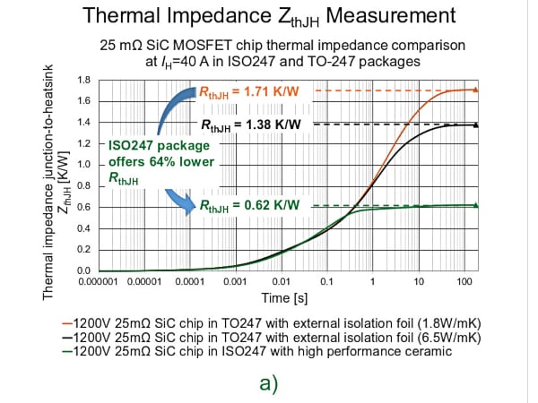
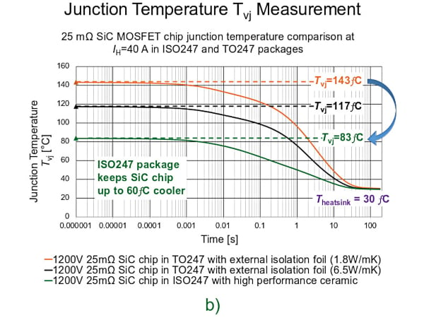
Figure 2. Comparison of a) thermal impedance and b) junction temperature measurement between ISO247 and TO-247 based SiC MOSFETs. Image used courtesy of Bodo’s Power Systems [PDF]
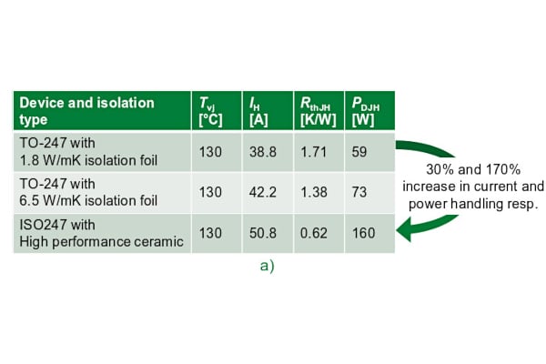
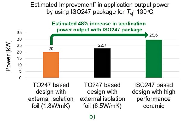
Figure 3. a) Thermal measurement results at Tvj=130°C and b) estimated increase in application power output by using ISO247. Image used courtesy of Bodo’s Power Systems [PDF]
The ISO247 solution additionally offers a considerable opportunity for cost savings (Table 2):
- Direct cost savings attributed to the enhancement in current and power handling capability, improved power density, savings in PCB area, and SiC chip cost
- Indirect cost savings due to reduction in potential warranty claims by eliminating isolation foil
Table 2. System-level cost savings opportunity using the ISO247.
|
Parameter |
*ISO247 solution |
TO-247 solution |
|
No. of devices |
6 |
12 |
|
No. of isolation pads |
Not Required |
12 |
|
Ease of assembly |
Simple |
Complex |
|
PCB area |
Up to 50% less area for ISO247 solution |
|
|
SiC chip cost |
Up to 50% savings for ISO247 solution due to the elimination of SiC device paralleling |
|
|
Dollar per Ampere ($/A) |
Up to 50% savings with ISO247 solution |
|
*Indicates potential for savings
Unique Packaging for WBG Devices
The growing prevalence of WBG devices demands innovative advancements in packaging technology to fully harness the advantages offered by WBG semiconductors. The ISO247 is a unique isolated package specifically designed to address the rigorous requirements of SiC-based applications while remaining compatible with the standard TO-247 footprint. From the thermal measurement comparison between the ISO247 and TO-247 packages, it has been established that the Littelfuse ISO247 with high-performance Si3N4 ceramic offers a remarkable 64% reduction in thermal resistance, RthJH and 53% reduction in temperature swing, ∆TJH. Consequently, the SiC MOSFET chip in the ISO247 package remains up to 60°C cooler at the same DC current. This significantly improves overall device lifetime and application reliability. In simpler terms, due to the improved thermal resistance, RthJH, and power dissipation, PDJH of the ISO247 package with high-performance ceramic, engineers can choose higher RDS(on) chips for a given application power rating. This presents a significant cost-saving opportunity at the system level. Additionally, employing the ISO247 in power-electronic applications reduces mounting efforts, enables space-saving, decreases overall thermal resistance, and increases power density, all while simplifying thermal design.
This article originally appeared in Bodo’s Power Systems [PDF] magazine.