Facebook
 Google
 GitHub
 Linkedin
Third Generation SiC MOSFETs for Highly Efficient EV Drivetrains
Learn how Bosch’s Gen3 SiC MOSFETs boost EV drivetrain performance. Its new trench architecture delivers 20% lower resistance and 10% lower switching losses, enhancing efficiency and reliability.
Article co-authored by Bosch's Samuel Araujo, Manuel Horvath, and Stephan Schwaige.
This article is published by EEPower as part of an exclusive digital content partnership with Bodo’s Power Systems.
The third generation of Bosch’s SiC MOSFETs stands out with its advanced trench design, yielding significantly optimized efficiency in electrified vehicle drivetrains. The new trench cell architecture effectively addresses the challenges posed by operation in the traction inverter. Improvements to the tradeoffs between conduction losses, switching losses, reliability, and robustness have optimized the power transistor for high efficiency and a long lifetime.
Advancing the Dual-Channel SiC Trench Gate MOSFET
Silicon carbide (SiC) trench MOSFETs are undisputedly the leading technology for automotive drivetrain inverters, which require high performance and robustness. As the demand for greater efficiency, power density, and reliability in electric vehicles continues to grow, Bosch is advancing the trench architecture to meet these needs.

Image used courtesy of Bodo’s Power Systems [PDF]
The Gen2 dual-channel design (see Figure 1) remains the foundation of this innovation. Its deep p-type shielding regions ensure optimal use of the trench architecture by utilizing both sides of the trench for on-state current conduction. This increases channel density, decreases resistance, and maximizes the active area for current flow, which is crucial for minimizing energy losses.
The deep p-type shielding implantations protect the gate complex in the trench and provide a common JFET region for both channels, limiting saturation current in the event of a short circuit. This intrinsic short-circuit protection is a vital safety feature that prevents thermal runaway and catastrophic failure under fault conditions.
Bosch has further advanced this concept with Gen3. By adding an extra shield implant to the trench itself (see Figure 1), the device is fully protected against off-state electric fields. During the off-state, the electric field experienced by the gate oxide is extremely low. Therefore, the off-state operation has no impact on the gate oxide’s lifetime. This improves the long-term reliability of the historically sensitive gate oxide.
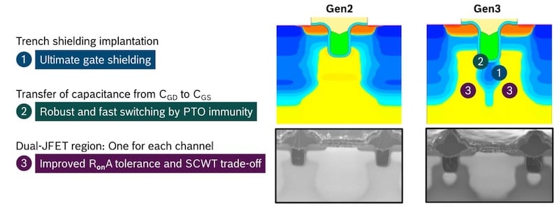
Figure 1. Advancing the dual-channel SiC trench gate MOSFET architecture from Gen2 to Gen3. Image used courtesy of Bodo’s Power Systems [PDF]
Gen3 SiC MOSFETs: Superior Performance, Robustness, and Heat Dissipation
The novel cell design improves static as well as dynamic performance, robustness, and heat dissipation (see Figure 2). A 20 percent reduction in specific on-resistance (RonA) significantly decreases the required chip area, resulting in more cost-effective converter designs with Gen3 devices (Figure 2, left). This directly translates to smaller and lighter power modules for electric vehicles (EVs).
Shifting part of the gate-drain capacitance (CGD) to the gate-source capacitance (CGS) reduces the gate-drain charge (QGD), achieving faster voltage commutation. Switching losses are reduced by about 10 percent during typical traction inverter operation, enhancing partial load efficiency and significantly improving the overall system efficiency
These performance improvements are achieved without compromising robustness. In fact, Gen3 enhances robustness against both short-circuits and parasitic turn-ons. This improvement is partially enabled by the newly implemented two-zone JFET region below the trench, which allows for more efficient current distribution during short-circuit events. In addition, decreasing the QGD lowers the Miller ratio.
A lower Miller ratio effectively damps gate voltage oscillations at the gate of the passive switch, thereby reducing the risk of parasitic turn-on. This allows for higher switching frequencies without compromising reliability. Consequently, switching speed can be safely increased. The short-circuit withstand time (SCWT) of Gen3 devices is about 10 percent higher than that of Gen2 trench MOSFETs (see Figure 2, right).
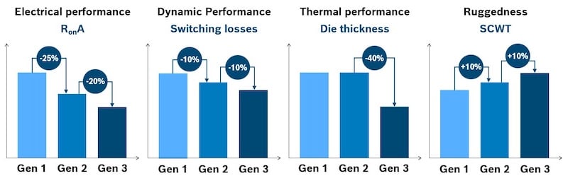
Figure 2. Gen3 outperforms Gen2 in terms of key performance metrics. Image used courtesy of Bodo’s Power Systems [PDF]
Finally, limiting the die thickness to 100 µm (Figure 2, middle) has a positive impact on thermal properties, leading to superior heat dissipation and enabling higher power densities.
A New Cell Architecture: Efficient Under Demanding Conditions
The new cell architecture was key to enhancing both robustness and performance. The narrower JFET regions and the one-to-one correspondence between channels and JFET regions greatly improved the trade-off between specific overall RonA and short-circuit withstand time. This balance is crucial, since improving one often degrades the other.
Although a narrower JFET naturally requires more processing, especially for lithographic alignment of the individual p-type regions, Gen3 elegantly circumvents this issue. Using a self-aligned implantation in the formed gate trench perfectly aligns the trench with its underlying protection implant, keeping the alignment tolerance at the same level as Gen2.
In other words, no new lithography layer is required to create additional protection implantation, and the existing hard mask of the trench etching process is reused, making mass production feasible and cost-effective.
The larger design window is reflected in Figure 3 (left), displaying the trade-off relationship between specific RonA and saturation current (Isat) during a short-circuit event. The entire trade-off curve is shifted in parallel, which yields a wider design space for robust and high-performing devices.
The device behavior during a short-circuit type 1 event (SC1, Figure 3, right) reflects the lower current density during the short-circuit condition, providing additional time for the gate driver to detect the fault and shut off the transistor. As a result, peak temperature as well as dissipated energy are significantly reduced, providing high intrinsic short-circuit robustness.
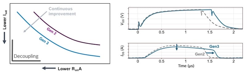
Figure 3. Compared with Gen2, the Gen3 SiC MOSFET device behavior shows a superior trade-off between specific on-resistance (RonA) and saturation current (Isat) during a short-circuit event. The transient gate-source voltage (VGS) and drain current (IDS) reflect a lower current density during the short-circuit event, as well as an extended time window for short-circuit detection and shutdown. Image used courtesy of Bodo’s Power Systems [PDF]
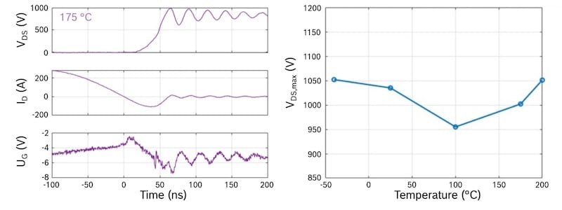
Figure 4. The reverse recovery behavior of the Gen3 SiC MOSFET body diode shows soft recovery with low voltage ringing. Transient drain-source voltage (VDS) and drain current (ID) versus time illustrate controlled current transition. Maximum reverse recovery voltage (VDS,max) versus junction temperature demonstrates stable operation across the temperature range. Image used courtesy of Bodo’s Power Systems [PDF]
For traction inverter operation in particular, a soft diode is important to reduce the current commutation slope for mitigating voltage peaks and high voltage commutation slopes during reverse recovery (Vrr). A “hard” recovery can result in damaging voltage spikes and increased electromagnetic interference (EMI). Gen3 body diodes are specifically designed to provide soft recovery behavior across the entire temperature range of -40 °C to 200 °C and a very high robustness against parasitic turn-on, especially at high temperatures, as shown in Figure 4 (left).
The body diode exhibits a very soft recovery behavior with controlled current decay (dI/dt), indicating gradual and well-controlled current transitions during reverse recovery. Only minimal voltage ringing is observed in the VDS waveform, indicating clean and fast switching behavior. Figure 4 (right) also illustrates high temperature stability by showing the maximum reverse recovery voltage (VDS,max) as a function of junction temperature (Tj).
Even at 200 °C, VDS, max remains well below 1,100 V – more than 400 V below the device’s breakdown voltage. This provides ample safety headroom, ensuring extremely reliable and safe operation under the most demanding switching conditions.
Conclusion
Bosch’s third-generation SiC MOSFETs represent a significant leap forward in power semiconductor technology for electric vehicle drivetrains. With its dual-channel trench architecture, enhanced by novel self-aligned shield implantations and refined JFET regions, these devices offer unmatched efficiency, robustness, and reliability.
Demonstrated improvements include a 20 percent reduction in specific on-resistance, a 10 percent decrease in switching losses, significantly enhanced short-circuit withstand capability, improved parasitic turn-on robustness, and a soft body diode that operates across a wide temperature range. These improvements collectively address the stringent demands of modern automotive applications.
By optimizing the RonASCWT trade-off and ensuring stable and safe operation under challenging conditions, Bosch’s Gen3 SiC MOSFETs maximize the performance and lifetime of EV inverters and contribute to the widespread adoption of high-performance electric vehicles. This continuous innovation underscores the critical role of advanced SiC technology in shaping the future of sustainable mobility.
This article originally appeared in Bodo’s Power Systems [PDF] magazine and is co-authored by Jens Baringhaus, Samuel Araujo, Manuel Horvath, and Stephan Schwaiger, Robert Bosch GmbH