Facebook
 Google
 GitHub
 Linkedin
Addressing SiC MOSFET Packaging Challenges
SiC MOSFET switching loss reduction is possible, but challenges exist in realizing high switching speeds during power module operation.
This article is published by EEPower as part of an exclusive digital content partnership with Bodo’s Power Systems.
The transition from power modules based on Si IGBT technology to power modules based on SiC MOSFET technology is inevitable. However, form factor preferences, which are carryovers from the Si IGBT era, still impede the commercialization of SiC technology as they have been known to have high parasitic inductance. Mitsubishi Electric has developed a modified NX package with an internal busbar structure suitable for SiC MOSFETs.
The Si IGBT chip technology has evolved, and the improvements gained from one chip generation to the next keep getting narrower (see Figure 1), indicating that each new generation is coming closer to the physical limits of the material itself.
Wide band gap semiconductors such as SiC MOSFETs offer the possibility of achieving a significant reduction in the overall semiconductor power losses. One aspect of the potential loss reduction using SiC MOSFETs comes from the possibility of reducing switching losses, increasing the switching frequency. As a result, the filter components can be optimized, and the corresponding losses would come down, leading to an overall reduction in the system losses.
![]()
Figure 1. Eoff versus VCE(sat) Comparison for various Si IGBT Generations. Image used courtesy of Bodo’s Power Systems [PDF]
The Challenge: SiC MOSFET Packaging Considerations
Switching loss reduction with SiC MOSFETs is possible because they can be switched much faster than Si IGBTs. However, certain challenges exist in realizing high switching speeds during the power module’s operation.
Switching overvoltage: The inductive voltage overshoot during turn-off of the MOSFET (∆VDS) is a function of the stray inductance (LS) of the power module package and the rate of change of drain current \((\frac{dI_{D}}{dt}.)\)
\[\Delta V_{DS}=-L_{S}\times\frac{dI_{D}}{dt}\]
![]()
Figure 2. VDS peak versus \(\frac{dI_{D}}{dt}.\) Image used courtesy of Bodo’s Power Systems [PDF]
![]()
Figure 3. Internal layout of the NX module (left), turn-on current waveform for the conventional NX module (right). Image used courtesy of Bodo’s Power Systems [PDF]
It can be inferred from Figure 2 that the higher the internal inductance of the package, the lower the maximum allowable \((\frac{dI_{D}}{dt}.)\).
Internal current balancing: A power module’s current rating depends on the number of individual dies that can be connected in parallel inside the package. Maintaining a homogenous distribution of drain current between the chips is important during static and dynamic operations. Therefore, the power module package has to be designed to ensure proper current balancing of the individual dies.
Form factor preference and challenges: Half bridge Si IGBT modules belonging to 650 V, 1200 V, or 1700 V classes having a rated current in the range of several hundred amperes are widely available in the NX package, which has established itself in the industrial power conversion segment for several years. Ideally, it would be advantageous to maintain the existing power module form factor (such as the established NX package). However, the conventional NX package has an internal inductance (LS) in the range of about 20 nH making it unsuitable for SiC adoption. In addition, as evident from the representation in Figure 3, the conventional NX package requires that the Si IGBT dies be placed along the long axis of the power module. As a result, the dynamic current sharing between the dies is not optimal and presents a challenge for direct SiC adoption.
Low Inductance NX Package for SiC Adoption
The internal layout of the NX package has been modified for SiC adoption. Figure 4 shows the modified NX package’s internal cross-section.
![]()
Figure 4. Internal cross-section of the modified NX package for SiC adoption. Image used courtesy of Bodo’s Power Systems [PDF]
The DC+ and DC- busbars are arranged in a ‘laminated structure’ placed as close to each other as possible (separated by an insulation layer) to maximize magnetic field compensation. In addition, the DC+ and DC- busbars are directly bonded to the substrate avoiding additional stray inductance by bond wire connections to the terminals. Furthermore, the dies are not placed along the long axis of the module (as was the case with the conventional NX design using Si IGBTs). An optimized circuit pattern has been developed (Figure 5) to achieve optimum current sharing between the different dies. The internal inductance of the modified low inductance NX module has been measured to be 9nH. This is around a 47% reduction of parasitic inductance compared to the conventional NX power module.
![]()
Figure 5. Internal layout of the modified NX package (left), turn-on current waveform for the modified NX package (right). Image used courtesy of Bodo’s Power Systems [PDF]
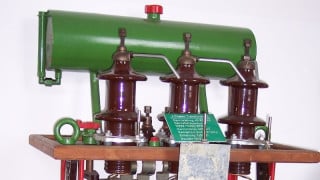
The NX SiC module has been released in the 1700V/600A rating (FMF600DXE-34BN) and 1200V/600A rating (FMF600DXE-24BN). Both devices have the half-bridge topology (2in1 configuration). The power module comprises a ceramic baseplate (AlN substrate) and utilizes silicon gel encapsulation. The power modules are based on Mitsubishi’s 2nd generation SiC chip technology.
![]()
Figure 6. A photo of the NX SiC module. Image used courtesy of Bodo’s Power Systems [PDF]
Performance Benchmarking
To understand the performance improvement using the modified SiC NX module, a benchmarking can be carried out considering the following items:
- Impact of the modified NX package (versus the conventional NX package)
- Performance benchmarking of the SiC MOSFET chip technology itself (versus Si IGBT technology)
Item 1 can be analyzed using the trade-off relationship shown in Figure 7—the inductive voltage overshoot (VDS [V] for SiC MOSFETs and VCE [V] for IGBTs) and the turn-off switching energy (Eoff [mJ/Pulse]). The following inferences can be obtained from Figure 7 considering the operation conditions DC-Link = 1000V, IC (or ID) = 600A, and Tvj = 150°C
a) Conventional NX package: The red curve indicates the VCE [V] for the 7th generation 1700V Si IGBT and the 1700V 2nd gen SiC MOSFET considering the conventional NX package (LS = ~ 20nH). It is possible to achieve lower turn-off losses (Eoff) using the SiC MOSFET in the same (conventional) package; however, the inductive voltage overshoot cannot be maintained within the RBSOA (Reverse Bias Safe Operating Area) with an adequate safety margin.
b) Modified low inductance NX package: The blue curve indicates the VDS for the 1700V SiC MOSFET considering the modified low inductance NX package. It can be seen that the RBSOA can be maintained at a safe limit without compromising the Eoff. Since the LS = 9nH, a lower turn-off gate resistance can be selected.
![]()
Figure 7. VDS peak versus Eoff for 2nd gen SiC considering the conventional NX package and the new low inductance NX package. 7th gen Si IGBT performance is included for reference. Image used courtesy of Bodo’s Power Systems [PDF]
Item 2 can be analyzed using Figure 8, which presents the power loss and junction temperature comparison of the 7th gen 1700 V Si IGBT (in the conventional NX package) and the 2nd gen SiC MOSFET (in both the conventional and the low inductance NX package). The conclusion from Figure 8 is that a 72% reduction in power losses versus the Si IGBT module is possible by adopting the modified low-inductance SiC MOSFET while maintaining the NX package outline. As a result, the switching frequency can be increased by a factor of 5 (enabling significant filter optimization) while keeping the maximum junction temperature below the maximum specified value.
![]()
Figure 8. Normalized power loss for 7th gen Si IGBT and 2nd gen SiC considering the conventional and the new low inductance NX package. Image used courtesy of Bodo’s Power Systems [PDF]
Better Power Loss Performance
To maintain a competitive edge and be economical for the end user, a certain level of efficiency and compactness becomes advantageous for every power conversion application. Each generation of Si IGBT has successfully displaced the previous generation with better power loss performance. As developments in Si IGBT technology reach saturation, SiC MOSFETs become more attractive. The last technical frontier for a full transition to SiC from Si is the form factor for power modules with Si IGBTs. The modified low inductance NX package and the 2nd generation SiC MOSFETs from Mitsubishi Electric aim to solve this and offer a viable solution for various power conversions.
This article originally appeared in Bodo’s Power Systems [PDF] magazine and is co-authored by Narender Lakshmanan and Eugen Stumpf of Mitsubishi Electric Europe B.V.