Facebook
 Google
 GitHub
 Linkedin
Comparing N-Channel and P-Channel MOSFETs
This article compares n-channel and p-channel power MOSFETs, introduces Littelfuse’s p-channel power MOSFETs, and explores target applications.
This article is published by EEPower as part of an exclusive digital content partnership with Bodo’s Power Systems.
Driving a high-side (HS) p-channel MOSFET without a charge pump or additional voltage source is easy, resulting in simplified design, space savings, reduced part count, and cost efficiency.

Image used courtesy of Adobe Stock
A Comparative Analysis of N-Channel and P-Channel Power MOSFETs
The cross-sectional view of the power MOSFET in Figure 1 illustrates the differences between n-channel and p-channel power MOSFETs. While an n-channel MOSFET requires a positive gate-source voltage to activate, a p-channel MOSFET needs a negative gate-source voltage. The key distinction lies in their reverse doping profiles: p-channel MOSFETs rely on holes as the majority charge carriers, generating hole current, while n-channel devices utilize electrons, creating electron current. Due to electrons’ superior mobility, which is roughly 2 to 3 times that of holes, moving holes in a p-channel device is more challenging than electrons in an n-channel device. This leads to higher area-specific on-state resistance in p-channel MOSFETs compared to n-channel MOSFETs. Consequently, achieving equivalent on-state resistance (RDS(on)) performance is impractical for p-channel MOSFETs of the same chip size as n-channel MOSFETs.
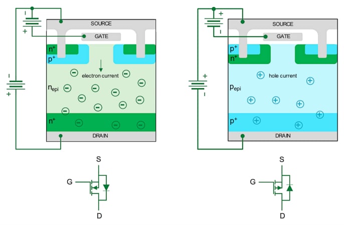
Figure 1. Cross sections of an n- and p-channel power MOSFETs with their symbols. Image used courtesy of Bodo’s Power Systems [PDF]
To achieve the same on-state resistance RDS(on) as the n-channel type MOSFET, the p-channel requires a 2 to 3-times larger die size. Therefore, in high-current applications, where low conduction losses are crucial, large die p-channel MOSFETs with very low RDS(on) are suboptimal. While the larger chip size of the p-channel device offers improved thermal performance, it exhibits larger intrinsic capacitances and higher switching losses. This drawback significantly impacts overall system cost, efficiency, and thermal management when the system operates at a high switching frequency.
In low-frequency applications with significant conduction losses, a p-channel MOSFET should match the RDS(on) of an n-channel MOSFET, requiring a larger chip area. Conversely, in high-frequency applications prioritizing switching losses, a p-channel MOSFET should align with the total gate charges of an n-channel counterpart, often having a similar chip size but a lower current rating. Therefore, choosing the right p-channel MOSFET demands careful consideration of device RDS(on) and gate charge (Qg) specifications along with the thermal performance.
Littelfuse P-Channel Power MOSFETs
Littelfuse p-channel power MOSFETs have traditionally served a limited range of applications. However, the recent increase in demand in low-voltage (LV) applications has broadened the scope of these p-channel power MOSFETs. The simplicity of Littelfuse p-channel solutions for HS applications makes them attractive for LV inverters (< 120 V) and non-isolated point-of-load solutions.
Littelfuse offers a range of industrial qualified p-channel power MOSFETs with the highest voltage class rating, lowest RDS(on) and Qg, high avalanche energy rating, excellent switching performance, and superior safe operating area (SOA) with best-in-class performance in both standard industrial and unique isolated packages. Littelfuse p-channel power MOSFETs retain the essential features of comparable n-channel power MOSFETs, such as fast switching, efficient gate-voltage control, and excellent temperature stability.
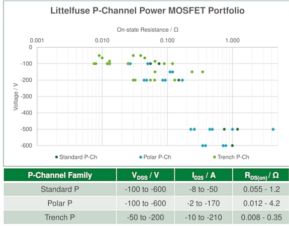
Figure 2. Littelfuse p-channel power MOSFET portfolio. Image used courtesy of Bodo’s Power Systems [PDF]
Figure 2 presents the key highlights of p-channel power MOSFETs offered by Littelfuse. Standard P and PolarP™ planar devices are available with voltage ratings from -100 V to -600 V and current ratings from -2 A to -170 A. PolarP™ offers optimized cell structure with low area-specific on-state resistance and improved switching performance, while Standard P benefits from a better SOA performance. Trench P utilizing a more dense trench gate cell structure offers very low RDS(on), low gate charge, fast body diode, and faster switching with device voltages ranging from -50 V to -200 V and currents from -10 A to -210 A. The latest addition to the portfolio is IXTY2P50PA (-500 V, -2 A, 4.2 Ω) which is Littelfuse’s first automotive grade p-channel power MOSFET for automotive applications.
Littelfuse p-channel power MOSFETs drive a broad range of industrial and automotive applications like battery and reverse polarity protection, HS load switches, DC-DC converters, onboard chargers, and LV inverters.
P-Channel MOSFETs in Half-Bridge Applications
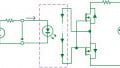
In typical half-bridge (HB) applications, n-channel MOSFETs are commonly used in the power stage. However, n-channel HS switches necessitate a bootstrap circuit to generate a gate voltage that is floating with reference to the source of the HS MOSFET or an isolated power supply to turn on as depicted in Figure 3a). Hence, the advantage of using n-channel devices comes at the cost of increased complexity in gate driver design leading to more design effort and greater space usage. Figure 3 illustrates the contrast between circuits using complementary MOSFETs and those using n-channel MOSFETs. When a p-channel MOSFET serves as the HS switch in this configuration as shown in Figure 3b), it can significantly simplify the driver design. A charge pump to drive the HS switch could be removed and the p-channel MOSFET can be easily controlled by the MCU through a simple level shifter. This reduces design effort and part count resulting in a cost-efficient design that utilizes space efficiently.

Figure 3. Simplification of the HS driver in HB application from a) N-channel MOSFET to b) p-channel MOSFET as HS switch. Image used courtesy of Bodo’s Power Systems [PDF]
Reverse Polarity Protection
Reverse polarity protection is a safety measure within systems to prevent potential fire hazards and damages in case of a reverse connection of the power source. Figure 4a) depicts the reverse polarity protection implemented using a p-channel power MOSFET. When the battery is correctly connected, the intrinsic body diode conducts until the MOSFET channel is activated. In the event of a reverse connection of the battery, the body diode is reverse-biased, with the gate and source at the same potential, thereby turning off the p-channel MOSFET. A Zener diode clamps the gate voltage of the p-channel MOSFET, safeguarding it in case of excessively high voltage levels.

Figure 4. a) Reverse polarity protection and b) Load switch using pchannel power MOSFET. Image used courtesy of Bodo’s Power Systems [PDF]
Load Switch
Load switches connect or disconnect a voltage rail to a specific load offering a cost-effective and simple way for a system to efficiently manage power. Figure 4b) demonstrates a circuit using a p-channel power MOSFET for a load switch. This circuit is driven by a logic enable (EN) signal to control the p-channel load switch via a small-signal n-channel MOSFET Q1. When EN is low, Q1 is off, and the p-channel gate is pulled up to VBAT. Conversely, when EN is high, Q1 activates, grounding the p-channel gate, and turning on the load switch. If VBAT exceeds the p-channel MOSFET’s threshold voltage, it can turn on when EN is high, eliminating the need for an additional voltage source to bias the gate, which is necessary for n-channel MOSFETs. The series resistor is needed to limit the current and a Zener Diode to clamp the gate voltage to a maximum value.
DC-DC Converters
In low-power DC-DC converters like the synchronous buck converter in Figure 5a), using a p-channel device as the HS switch simplifies the circuit and saves space, eliminating the need for external gate driving circuitry. It also reduces the bill-of-materials (BOM), leading to cost efficiency. Similarly, in synchronous boost converters, a P-channel device can replace a diode with low forward voltage as an output synchronous rectifier, as seen in Figure 5b). This improves the converter efficiency due to the improved figure-of-merit (FoM = RDS(on) * Qg) of the p-channel MOSFET.

Figure 5. Low power a) synchronous buck and b) synchronous boost converter using complementary MOSFETs. Image used courtesy of Bodo’s Power Systems [PDF]
P-Channel MOSFETs in Low-Voltage Applications
As modern LV applications advance, Littelfuse’s p-channel power MOSFETs prove their versatility in meeting the evolving needs of today’s power electronics. Employing Littelfuse’s p-channel MOSFETs provides designers with simplified, more reliable, and optimized circuit design in industrial and automotive applications. To achieve optimal performance for specific applications, designers must assess the trade-off between RDS(on) and Qg when selecting a p-channel power MOSFET.
This article originally appeared in Bodo’s Power Systems [PDF] magazine and is co-authored by Sachin Shridhar Paradkar, Raymon Zhou, and José Padilla of Littelfuse.