Facebook
 Google
 GitHub
 Linkedin
Rethinking Soft-Switching Efficiency With Silicon Carbide
This article examines how silicon carbide differs from silicon, and how circuit techniques such as soft switching can be optimized beyond what is practical with silicon.
This article is published by EEPower as part of an exclusive digital content partnership with Bodo’s Power Systems.
On paper, silicon carbide (SiC) technology has advantages over silicon (Si) that make it seem like it can be used as a drop-in replacement for existing MOSFETs in power electronics. That is true to some extent, but it is possible to obtain much more from SiC by paying attention to the ways the technology differs from silicon and how circuit techniques, such as soft switching, can be optimized beyond what is practical with silicon.
SiC’s wider bandgap compared to silicon results in higher breakdown voltage and electron mobility, which together reduce onstate resistance. It also enables faster switching speeds compared to silicon, resulting in improved efficiency and the ability to design power electronics systems with smaller form factors. SiC also has a thermal conductivity significantly higher than silicon, allowing for the design of power electronics devices that can operate at higher temperatures without sacrificing performance or reliability.
Image used courtesy of Adobe Stock
Whereas circuits based on conventional silicon superjunction MOSFETs need only take account of simple soft-switching techniques, the higher typical frequency of operation means SiC benefits from a careful analysis of when and where losses occur. In turn, that analysis can lead to novel solutions that avoid losses that are inherent to conventional MOSFET-based circuit designs.
For example, a key advantage of a wide-bandgap technology like SiC is the ability to guarantee a higher breakdown voltage for a given on-state resistance. This allows the use of a thinner drift layer that presents less resistance compared to the thicker layers needed for bulk-silicon devices. At the same time, the composition of the crystal lattice delivers higher carrier mobility. The net result is considerably higher conductivity.
The junction field-effect transistor (JFET) is the best option to minimize drain-source resistance. In a MOSFET, the carriers must pass across the surface of the p-base (p-well) region through a resistive inversion channel at the MOS interface before entering the n-type drift region. However, in a JFET, there is no such inversion channel. By using a high bulk majority carrier mobility, the JFET approaches the theoretical limit of on-state resistance compared to breakdown voltage. Qorvo’s SiC JFET-based devices allow a transistor design with a greater safety margin on breakdown voltage compared to MOSFET designs and an on-state resistance nearly half that of competing parts.
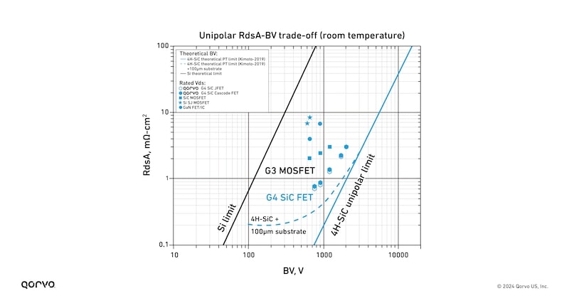
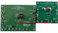
Figure 1. Qorvo’s Gen4 SiC FETs exhibit roughly half the RdsA of traditional SiC MOSFETs. Image used courtesy of Bodo’s Power Systems [PDF]
Conventionally, using a depletion mode JFET on its own introduces circuit design challenges. As a normally-on device, it needs a negative voltage to turn off completely. However, SiC MOSFETs have low threshold voltages, so negative gate voltages are not uncommon in real-world circuits. Applying negative voltages prevents the accidental turn-on of the transistors at temperature extremes where the threshold voltage may drop below nominal levels.
Qorvo’s solution combines a SiC JFET with a low-voltage silicon MOSFET in a cascode structure where the SiC JFET gate-to-source voltage is the inverse of the Si MOSFET drain-to-source voltage. This cascode structure is illustrated in Figure 2. In the cascode configuration, the external gate drive controls a low-voltage Si MOSFET drain-to-source voltage, which indirectly drives the high-voltage SiC JFET. This cascode configuration provides control familiar to engineers used to working with silicon super-junction MOSFETs. The lower operating voltage of the MOSFET contributes less than 10% to the overall on-state resistance of the pair of devices. To aid integration, Qorvo supplies this configuration in a single package.
The cascode structures provide control over switching through the Si low-voltage MOSFET, decoupling the control logic from the high-voltage JFET. Such a decoupling provides the opportunity to optimize the gate control voltage range and gate charge for the low-voltage Si MOSFET without sacrificing the full performance advantages of the SiC JFET. Unlike conventional SiC MOSFETs that typically require gate voltage as high as 18 V to fully activate the device and achieve the full benefit of low on-state resistance, the cascode architecture allows lower maximum gate-control voltages and eliminates the need for negative voltages in the off-state. This narrowing of the voltage range reduces gate charge by 50% (from 18 V/-4 V to 10 V/0 V), potentially reducing losses during switching, particularly for soft-switching applications at light loads.
Switching to SiC with a JFET structure significantly shrinks die size. Qorvo’s device has an almost ten-fold reduction in die area with the same power-handling ability as silicon super-junction devices. SiC’s thermal conductivity and superior efficiency offset the increase in thermal resistance that accompanies a significantly smaller die. Any further increases in thermal resistance are offset through the use of silver sintering for die attach, which provides a six-fold improvement in thermal conductivity compared to conventional solders.
The application of a cascode structure to a SiC JFET further improves efficiency by reducing stray capacitances that affect silicon super-junction devices and SiC MOSFETs. The lower stray capacitances also improve density by driving the switching frequency higher than is practical with silicon devices and even SiC MOSFETs.
The benefits are most apparent in soft-switching circuit architectures. While soft-switching techniques used with silicon devices tackle some of the most obvious sources of loss due to the turn-on and turn-off phases of the switching cycle, the fast-switching capability of the latest generation of SiC transistors addresses more subtle issues that are generally missed.

Figure 2. Cross-section view of planar SiC MOSFET (left) and Qorvo cascode SiC FET (right). The dominant channel resistance (Rchannel) of SiC MOSFET is replaced by a much lower RDS(on) low-voltage Si MOSFET in a cascode structure. Image used courtesy of Bodo’s Power Systems [PDF]
Many circuits based on silicon devices employ zero-voltage switching (ZVS). Its primary purpose is to reduce the voltage between the drain and source during the transistor turn-on transition before the current begins to flow freely through the transistor channel. Ideally, the device drain-to-source current (IDS) and drain-to-source voltage (VDS) have almost zero overlap, thus eliminating turn-on switching loss. The output capacitance (i.e., the sum of the drain-source capacitance and the capacitance between the gate and drain) is normally fully charged to the DC link bus voltage during device turnoff in the previous cycle and is recycled into the load to avoid losses during the next ZVS turn-on event.
ZVS turn-on with a conventional Si device can lead to a period of dead time in the switching cycle that can last as long as 300 ns due to the high output capacitance of silicon devices. At a switching frequency of 500 kHz (2 µs period), a 300 ns dead-time during both turn-on and turn-off transitions represents 30% of the duty cycle. The SiC JFET delivers a key advantage over Si MOSFETs because it has 10x lower output capacitance that takes less time to clear, especially at low drain-to-source voltage bias where output capacitance increases significantly for Si MOSFETs. Silicon super-junction devices have strong nonlinearity in the CV curve at low drain-to-source voltage bias, which leads to high voltage transition time near the bus voltage and 0V during the switching transition in a half-bridge topology. This reduces the length of the dead time needed for ZVS, which can be traded for higher-frequency operation or more power delivered to the load.
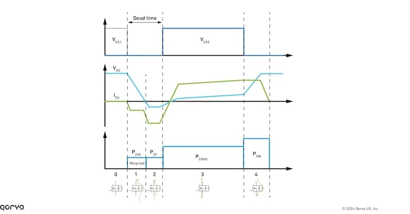
Figure 3. Illustration of key waveforms and loss distribution in ZVS soft switching applications. Image used courtesy of Bodo’s Power Systems [PDF]
Due to the long voltage transition time and relatively high turn-off switching loss, designs for ZVS circuits using Si devices are limited to switching frequencies below 150 kHz. With the fast-switching capability of the Qorvo SiC FET, the switching frequency boundary is pushed beyond 500 kHz. Similar to turn-on switching loss, efficiency improves if the overlap between the fall in current and the rise in drain-source voltage during turn-off is minimized.
However, EMI becomes more challenging with increased switching speed. Designers must diligently minimize PCB parasitics from critical current commutation loops early in the design phase to fully exploit SiC’s fast-switching capability. However, there is a limit on how much optimization can be achieved when safety requirements (e.g., clearance, creepage, etc.) are considered. Once the circuit design is finalized, there are two popular ways to further fine-tune turn-off drain-to-source voltage spikes and ringing. One is using high gate resistance (Rg) to slow device switching speed. A more effective and efficient way is to use a snubber circuit, as shown in Figure 4, with low gate resistance. In other words, use small gate resistance to allow fast switching of SiC devices, and use snubber RC to control VDS spikes and ringing. The device snubber Cs provides VDS peak overshoot control while Cd minimizes power loop stray inductances by being placed close to the fast-switching half-bridge. Rs and Rd provide damping for VDS ringing.
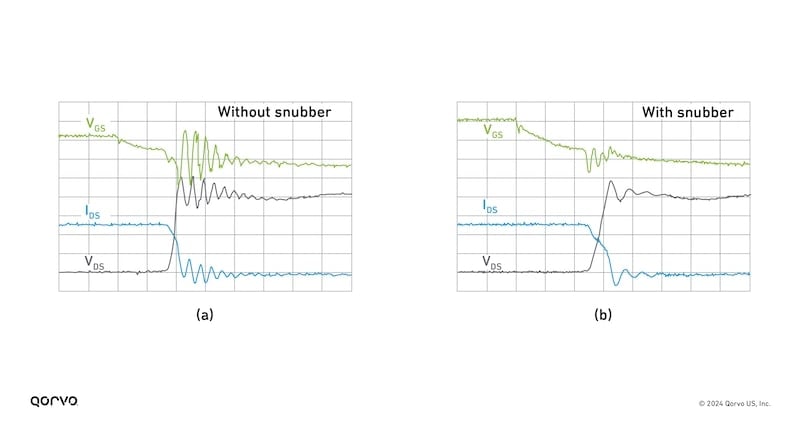
Figure 4. DPT schematic with an RC snubber on both switches for (a) hard-switching and (b) ZVS soft-switching. Image used courtesy of Bodo’s Power Systems [PDF]
A common misconception is that using a snubber is inefficient. For a half-bridge topology—typically used in ZVS applications such as LLC or PSFB—using a snubber is much more efficient than using high gate resistance because the added drain-to-source capacitor does not generate any turn-on loss. During the turn-off dv/dt phase, the displacement current of the freewheeling device will further decrease the turn-off current of the device that has been actively turned off, thus reducing voltage and current overlap to greatly reduce turn-off loss (Eoff). The displacement current level is determined by the equation I = C*dv/dt. C is the equivalent output capacitance and includes both device output capacitance (Coss), and the extra snubber Cs paralleled across the device drain-to-source. With extra snubber capacitance between the drain and source and high dv/dt (i.e., low gate resistance), the displacement current will be higher. This leaves less current to overlap with VDS for the active turn-off device, thus reducing turn-off switching loss. This approach allows us to contain the VDS ringing and spikes without sacrificing as much device switching speed had we instead used a high Rg solution. Figure 5 shows double pulse test turn-off waveforms, with and without a snubber, to intuitively demonstrate that using a snubber with low gate resistance greatly reduces the voltage and current overlap, which in turn reduces turn-off switching loss.
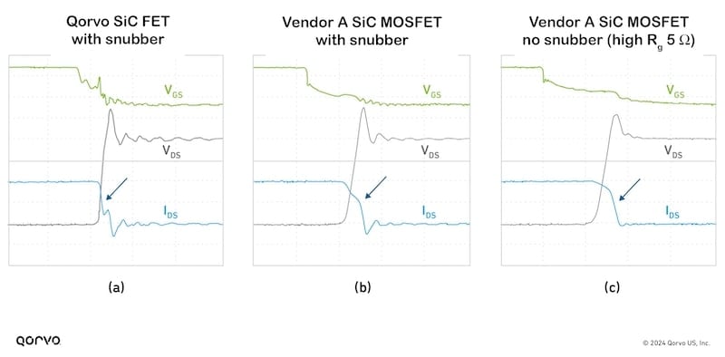
Figure 5. 800V VDS, 100A IDS turn-off waveforms for Qorvo’s SiC modules in E1B packaging: (a) UHB100SC12E1BC3-N (1200V, 100A E1B module) with snubber (660pF, 4.7Ω, Rgoff 2.2Ω), (b) Vendor A 1200V, 100A SiC module with snubber (660pF, 4.7Ω, Rgoff 2.2Ω), (c) Vendor A 1200V, 100A SiC module without snubber (Rgoff 5Ω). Image used courtesy of Bodo’s Power Systems [PDF]
The savings possible through the use of snubbers emphasize the importance of leveraging soft-switching circuit architectures when using SiC to maximize efficiency. Snubber circuits present less of a benefit in hard-switching designs, where the energy stored in Cs from the turn-off cycle is often wasted as heat in the device channel during the next turn-on cycle. However, even with this turn-on loss penalty of using a snubber, the overall switching loss (i.e., the sum of turn-on and turn-off switching losses) is still much lower than simply using high gate resistance at full load (i.e., the device’s rated current level).
Referencing the waveforms from Figure 5 for a double pulse test conducted with an 800 V bus voltage and 100A load current, the analysis summarized in Figure 6 reveals that adding snubber results in a 50% reduction in losses for the SiC MOSFET module from vendor A. The combination of using Qorvo’s JFET-based devices with a snubber delivers an additional 74% reduction in turn-off switching loss. This makes it possible to increase the switching rate threefold and drive a reduction in the size of external passive components. Citing the simulation of a 50 kW PSFB (phase-shifted full bridge), the 74% reduction in turn-off switching loss also helps drive a 10% reduction in junction temperature (Figure 7). Ultimately, better thermal performance leads to smaller heatsinks and cooling structures; combined, the two translate into a reduction in converter volume.
Though SiC has inherent advantages over silicon in power-electronics design, reassess both device selection and circuit topology to gain the best performance possible. Fast switching coupled with the combination of a snubber circuit and the inherent low drain-to-source resistance of the Qorvo SiC cascode JFET configuration enables dramatic leaps in efficiency and power density for ZVS soft switching applications
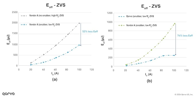
Figure 6. DPT test results at 800V VDS, 100A IDS for turn-off switching loss for Qorvo SiC modules in E1B packaging: (a) Vendor A 1200 V, 100 A SiC module with snubber (660 pF, 4.7 Ω, Rgoff 2.2 Ω) and without snubber (Rgoff 5 Ω), (b) Qorvo UHB100SC12E1BC3-N (1200 V, 100 A SiC module in E1B packaging) with snubber (660 pF, 4.7 Ω, Rgoff 2.2 Ω) and Vendor A with snubber (660 pF, 4.7 Ω, Rgoff 2.2 Ω). Image used courtesy of Bodo’s Power Systems [PDF]
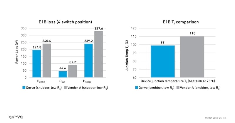
Figure 7. FET loss from simulation of a 50 kW phase-shifted full bridge. Application conditions: 50 kW, 800 V VIN, 400 V VOUT, 150 kHz, deadtime 150 ns, heatsink temp 75°C. Image used courtesy of Bodo’s Power Systems [PDF]
This article originally appeared in Bodo’s Power Systems [PDF] magazine.