Facebook
 Google
 GitHub
 Linkedin
Improving Reverse Recovery Time With Trench MOS Structures
Trench MOS structures offer several benefits compared to traditional p-n junction solutions. Learn what they are here.
This article is published by EEPower as part of an exclusive digital content partnership with Bodo’s Power Systems.
Schottky Barrier Diodes (SBD) have several key features that differentiate them from p-n junction diodes. First is how they are constructed: In p-n junction diodes, the junction is formed between p-type and n-type semiconductor materials, whereas SBDs have a metal-semiconductor junction. Because the metal-semiconductor junction has a smaller barrier for the current flow compared to p-n junction diodes, they have a lower forward voltage drop (lower VF). This, in turn, leads to faster and more efficient switching, making SBDs a good choice for high-frequency applications such as power supplies and rectifiers. SBDs also have a higher reverse leakage current than p-n junction diodes and have almost zero TRR (reverse recovery time), allowing them to quickly switch between conducting and non-conducting.

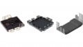
Figure 1. The YQ Schottky Barrier Diodes (SBD) lineup offers options for a variety of applications from automotive to industrial. Image used courtesy of Bodo’s Power Systems [PDF]
Schottky diodes are often used in applications where fast switching speeds, low forward voltage drop, and low reverse recovery time are critical — such as rectification, clamping, and protection circuits in power supplies, voltage regulators, and RF circuits. The major issue for SBDs involves heat temperature sensitivity, as their forward voltage drop increases with temperature due to the generated heat, leading to problematic inefficiencies.
Trench MOS Structure
The two basic types of MOS (Metal-Oxide Semiconductor) structures used for SBDs are planar and trench, as compared in Figure 2. In general, trench MOS structures (compared to planar structures) exhibit low resistance in the epitaxial wafer layer during forward bias, leading to low VF. During reverse bias, IR is reduced because the electric field concentration is mitigated.
The planar MOS structure comprises a metal layer, a Schottky metal layer, and an oxide film over an N- epitaxial layer on top of an N+ substrate wafer, all stacked on one another. The trench MOS structure comprises a metal layer on top of a Schottky metal layer. Beneath is the epitaxial layer with trenches enclosed within an oxide film containing a polysilicon layer. Beneath the epitaxial N-layer is the substrate layer.
Figure 2 illustrates the electric field distribution when applied in the reverse direction. In the traditional planar structure, the electric field is concentrated at the metal junction; however, Rohm’s proprietary trench structure mitigates the electric field concentration with the highest field strength occurring where the oxide film contacts the epitaxial N-layer. When applied in the reverse direction, the electric field concentration is unlikely. The epitaxial layer exhibits low IR even with low resistance; when applied in the forward direction, it exhibits low resistance, and a lower VF is achieved, leading to higher efficiencies in rectification applications.
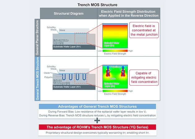
Figure 2. Comparing the planar MOS structure to the trench MOS structure. Image used courtesy of Bodo’s Power Systems [PDF]
YQ Series Schottky Barrier Diodes
Rohm has introduced the YQ series SBD with a 100 V breakdown for power supply and protection circuits in automotive, industrial, and consumer applications. As Figure 3 illustrates, the YQ series is part of the Rohm power SBD lineup.
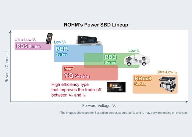
Figure 3. Rohm’s power SBD lineup, including the YQ series. Image used courtesy of Bodo’s Power Systems [PDF]
Rohm’s proprietary trench MOS structure simultaneously reduces VF and IR for reduced power losses, including reduced loss when used in forward bias applications. The overall switching loss is reduced by approximately 26% compared to general trench-type MOS products. They also exhibit a class-leading TRR of 15 ns, reducing TRR loss by about 37% when switching applications. The YQ series also runs less risk of thermal runaway.
Performance
The SBDs have a reputation for greater miniaturization, lower losses in applications for the automotive, industrial, and consumer equipment markets, and reduced VF and IR. The YQ series achieves a class-leading TRR of 15 ns compared to 19 ns for standard trench MOS products (IF of 3 A and VR of 48 V), as shown in Figure 4. Note that this was for IF = 3 A, VR = 48 V, and di/dt = -200 A/µs.
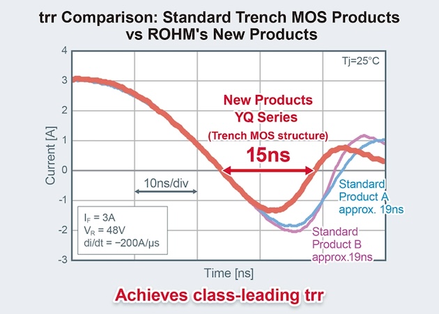
Figure 4. Comparing the TRR of the YQ series to two equivalent power SBD solutions. Image used courtesy of Bodo’s Power Systems [PDF]
Figures C and D compare the results of the IF-VF and capacitance-VR characteristics for the TO-277 package products in the 100V/10A class for the YQ10RSM10SD and the equivalent power SBDs from three other companies.
Figure 5 shows that the YQ10RSM10SD has one of the lowest VF characteristics, nearly equivalent to the company A product, which implies that these two SBDs have the lowest conduction loss. In contrast, the VF of companies B and C products are higher by approximately 10-20%, leading to higher conduction losses than the YQ10RSM10SD and company A.
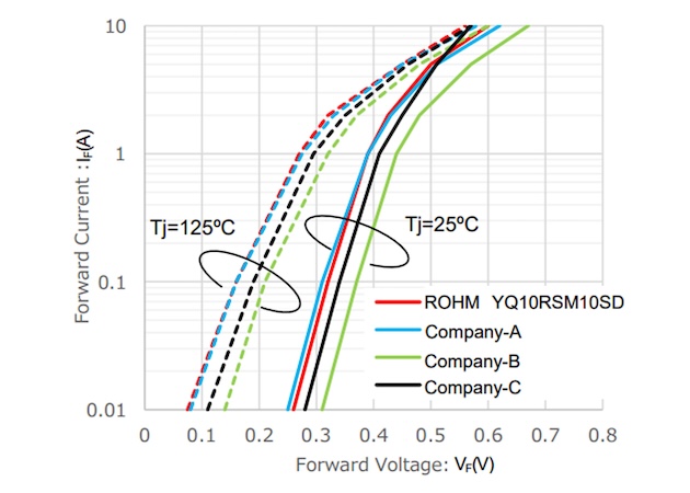
Figure 5. Forward current vs. forward voltage for the YQ10RSM10SD compared to three other equivalent SBD solutions. Image used courtesy of Bodo’s Power Systems [PDF]
Based on the capacitance VR characteristics shown in Figure 6, the YQ10RSM10SD has the lowest switching loss due to having the smallest capacitance (approximately half) compared to products A, B, and C.
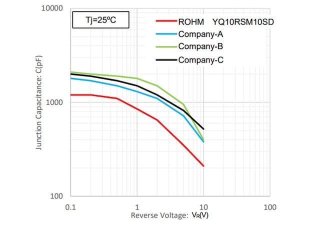
Figure 6. Junction capacitance vs. reverse voltage for the YQ10RSM10SD compared to three other equivalent SBD solutions. Image used courtesy of Bodo’s Power Systems [PDF]
Technical Specifications
Figure 7 shows the YQ lineup based on packaging and summarizes key technical specifications.
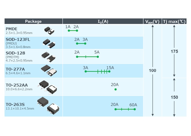
Figure 7. The YQ SBDs lineup. Image used courtesy of Bodo’s Power Systems [PDF]
Use Case: Automotive Headlamps
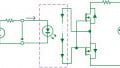
There are numerous applications for the YQ series SBDs, including automotive LED headlamps, xEV DC-DC converters, power supplies for industrial equipment, and lighting. One common application f is rectifying the boost block in the peripheral circuitry of automotive LED headlamps. The circuitry is shown in Figure 8, where the SBD power MOS is outlined in red, the boost block in yellow, and the low-side switch block in blue.
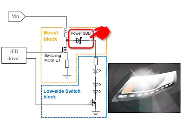
Figure 8. Circuit for rectifying the boost block in the peripheral circuitry of automotive LED headlamps. Image used courtesy of Bodo’s Power Systems [PDF]
Such circuits for automotive LED headlamps are energized under a sealed condition, meaning temperatures can become very high. To further complicate matters, the number of bulbs in automotive headlamps has increased, and the size of circuit boards has decreased in recent years, leading to harsh heat generation conditions and very high temperatures.
A power SBD for this type of application should exhibit low VF and IR with excellent heat dissipation to reduce the possibility of thermal runaway risk, which is what the YQ power SBD achieves.
Using the automotive LED driver BD18353EFV-M and its evaluation board, as shown in Figure 9, the power conversion efficiency and heat generation of a YQ10RSM10SD (100 V/10 A/TO-277) were compared to similar products from other companies. Figure 9 outlines the switching MOSFET in blue, and an RD3P100SNFRA (100V/10A/TO-252) was used.
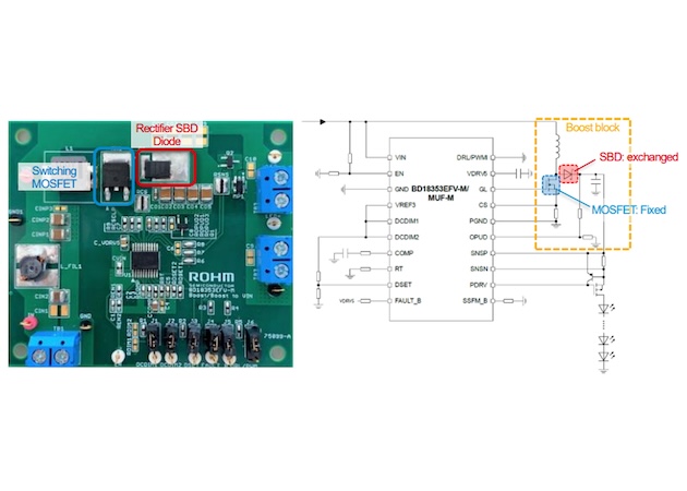
Figure 9. Picture of the evaluation board and circuit diagram. Image used courtesy of Bodo’s Power Systems [PDF]
Figure 10 shows the evaluation board and circuitry used. This evaluation was performed by exchanging the rectifier diode, outlined in red, in the boost block. Based on results from the LED Headlamp evaluation board, when a standard trench MOS product is compared to the YQ series product (see Figure 10), the TRR loss is reduced by approximately 37%, and the switching loss is reduced by 26%.
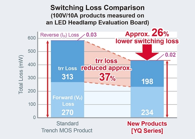
Figure 10. Switching loss comparison measured on an LED headlamp evaluation board. Image used courtesy of Bodo’s Power Systems [PDF]
Figure 11 shows the efficiency and package surface temperature Tc results. First, it was confirmed that YQ10RSM10SD (with excellent VF and capacitance characteristics) has the highest power conversion efficiency and keeps Tc the lowest at 55.8°C. The efficiency of B and C are significantly lower, and the Tc is significantly higher at 61.0°C and 59.2°C, respectively, even with the same package, due to a high VF. Even though A has a VF characteristic equivalent to the YQ10RSM10SD, efficiency is lower, and Tc (58.0°C) is higher because of its higher switching losses.
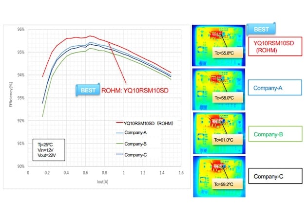
Figure 11. Comparison results of the efficiency and package surface temperature using the YQ10RSM10SD to an equivalent solution from three other companies, A, B, and C. Image used courtesy of Bodo’s Power Systems [PDF]
The YQ SBD series has a proprietary trench MOS structure that offers several benefits over traditional p-n junction solutions. One is a tradeoff between IR and VF that leads to better efficiency and less heat generation. These 100 V breakdown Schottky Barrier Diodes provide industry-leading TRR and are ideal for protection and power supply circuits used in industrial, automotive, and consumer applications.
This article originally appeared in Bodo’s Power Systems [PDF] magazine. Featured image used courtesy of Adobe Stock.