Facebook
 Google
 GitHub
 Linkedin
Navitas Launches 5th-Gen 1200 V GeneSiC TAP SiC MOSFETs
The 5th-gen 1200 V trench-assisted planar SiC MOSFETs offer 35% FoM improvement, improved switching behavior, and extended reliability testing.
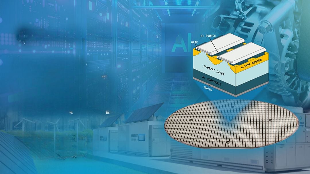
Navitas Semiconductor has introduced its 5th-generation GeneSiC trench-assisted planar (TAP) silicon carbide (SiC) MOSFET technology platform, led by a 1200 V product line. These new MOSFETS were designed to target high-voltage power conversion in AI data centers, grid and energy infrastructure, and industrial electrification.
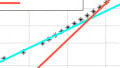
When compared to the previous 1200 V generations, the 5th gen GeneSic MOSFET platform has delivered up to a 35% improvement in the RDS(on) × QGD figure of merit. That metric directly affects both conduction and switching losses, making it particularly relevant in high-frequency, high-density power stages.
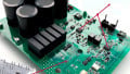
The 5th-generation GeneSiC trench-assisted planar SiC MOSFET. Image used courtesy of Navitas Semiconductor
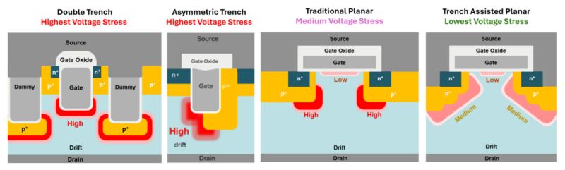
Why the Trench Matters
Navitas’ trench-assisted planar structure blends a primarily planar gate with shallow-trench features in the source region. Unlike full trench MOSFETs, those trenches do not form the main current channel. Instead, they are introduced to shape electric field distribution and improve current spreading inside the device.

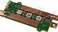
Cross-sectional comparison of planar SiC MOSFET structures. Image used courtesy of Navitas Semiconductors
In high-voltage SiC devices, concentrated electric fields can create reliability issues, especially around the gate oxide. This design distributes the electrical stress more evenly, improving long-term durability without the added manufacturing complexity of deep trench structures. The structure also helps keep RDS(on) lower at higher temperatures. Since on-resistance increases as devices heat up, keeping it more stable across the operating range helps reduce conduction losses and improve overall thermal performance in high-power converters.
Cutting Switching Losses Where It Counts
The 35% improvement in RDS(on) × QGD is central to this generation. Lower RDS(on) reduces conduction losses, while lower gate-drain charge reduces the energy required during voltage transitions. In high-frequency power supplies and inverter stages, those reductions could translate into lower heat and higher achievable power density.
Comparing current spreading across planar SiC MOSFET designs. Image used courtesy of Navitas Semiconductor
Navitas reports a 25% improvement in the QGD/QGS ratio. With a threshold voltage of VGS,TH ≥ 3 V, the platform is built to prevent parasitic turn-on in high dV/dt switching environments. As switching speeds increase, having stable gate behavior becomes more important.
The new 5th generation was designed to improve dynamic performance by optimizing the RDS(on) × EOSS characteristic, which can reduce overall energy loss during switching transitions. The integrated “soft body-diode” design also supports smoother current commutation and helps lower electromagnetic interference during hard-switching operation.
Built for High-Stress Environments
Reliability qualification is the 5th-generation platform’s major focus, as Navitas classifies the devices as “AEC-Plus” grade, exceeding AEC-Q101 and JEDEC standards based on internal test results.
Navitas reports that extended high-temperature reverse-bias and high-temperature gate-bias testing was conducted for durations up to three times longer than standard qualification requirements, along with dynamic reverse-bias and dynamic gate-switching tests designed to reflect real fast-switching conditions in data center and grid applications. The company also cites that, with minimal threshold voltage shift under prolonged switching stress, an extrapolated gate-oxide failure time can exceed one million years at 18 V gate bias and 175°C.
The 1200 V 5th-generation devices complement Navitas’ existing 2300 V and 3300 V ultra-high-voltage GeneSiC offerings, broadening the company’s SiC portfolio across multiple voltage classes. With better switching performance, improved high-temperature stability, and expanded reliability testing, the 5th generation GeneSIC trench-assisted planar MOSFET is built for high-voltage systems that need to run efficiently, manage heat effectively, and operate reliably over long periods.