Facebook
 Google
 GitHub
 Linkedin
An Inside Look at New-Gen MOSFETs and the Future of SiC vs. GaN
Alfred Vollmer of Bodo's Power Systems spoke with Sanan Semiconductor's Michael Sleven for a look at new MOSFET technology and what the future holds for SiC and GaN.
This article is published by EEPower as part of an exclusive digital content partnership with Bodo’s Power Systems.
Sanan Semiconductor has moved from a pure foundry to a vertically integrated full-service semiconductor design and production company that also ships automotive-qualified components. Alfred Vollmer of Bodo’s Power Systems spoke with Michael Sleven, Vice President of Sales Europe at Sanan Semiconductor, about new MOSFETs and a joint venture, megafabs, and what the future holds for SiC and GaN.
Alfred Vollmer: Sanan is launching its third generation of SiC MOSFETs. What technical features can we expect?
Michael Sleven: We will launch more MOSFETs in our Gen 2 and new Gen 3 trench-structured SiC MOSFETs throughout 2024. We will have a complete portfolio fulfilling AEC Q101 standards for industrial and automotive applications. With our matured wafer thinning platform of 120 µm, we are using heavily doped n-substrates. The devices show high current density and very low losses. The tradeoff between Ronsp (mΩ/mm2) and cell pitch (µm) is absolutely competitive. Besides the MOSFETs, we have completed our SBD portfolio. In addition to our Gen 3 SBDs for general power applications, we have started to serve our Gen 4 with very low Vf and Gen 5 with an increased surge current capability.
Image used courtesy of Adobe Stock
Vollmer: Sanan and STMicroelectronics have announced a SiC cooperation. What can we expect from this collaboration?
Sleven: As part of this joint venture, we built another vertical inline megafab combined with an investment of $3.2 billion. This plant will start mass production by the end of 2025 and will serve around 520,000 8-inch wafers exclusively for ST Microelectronics in 2028. This JV is a major step to establish Sanan further as a reliable and innovative partner for high-quality compound semiconductors. In addition to the new fab for ST in Chongqing, we have the Mega Fabs in Xiamen and Quanzhou with a monthly production capacity of 30,000 wafers each. Our newest fab in Changsha has a production capacity of 360,000 6-inch and 400,000 8-inch wafers per year. We are prepared to start the production with 8-inch wafers for GaN if needed. So, we are very well prepared to feed the market demand.
Vollmer: Sanan Semiconductor is active in SiC and GaN semiconductors. What are your core competencies?
Sleven: Sanan Semiconductor has more than 20 years of experience with compound semiconductors and different materials, especially for automotive applications. We deliver huge quantities in stable quality from our megafabs. In the recent past, we have started a tensioned journey to increase our portfolio with final discrete and module packages in addition to our business as a foundry. We have more than 350 patents only with SiC applications on hand, so our degree of innovation is one of our core competencies.
We have one of the biggest vertical inline SiC factories in the world, covering substrate materials, epitaxial growth, chip manufacturing, packaging, testing, and other sections. Our GaN products are made on our own SiC substrates. So, we have every process step in our own hands. This makes us fast and able to offer attractive prices to our customers. The huge production capacities of Sanan allow a stable supply.
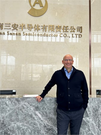
Michael Sleven, Vice President of Sales Europe, Sanan Semiconductor. Image used courtesy of Bodo’s Power Systems [PDF]
Vollmer: How do you expect the automotive market to develop?
Sleven: The compound semiconductor market has changed completely during the last few years. In automotive, we have a high dynamic combined with strong requirements for higher current densities and cost reductions. Today we are serving most of our SiC parts to OEMs and Tiers, and the growth potential for the next years is incredibly high. For onboard chargers and drivetrain inverters SiC is the best choice today. To increase our business in Europe, we have established a new experienced team for the European market to support our customers deeply with calculations and simulations to define the right technologies and parts. Our FAEs have a good system knowledge of the applications, and the short response time from our team is also key to our success. The automotive market will be the biggest market in the future, and so at Sanan, we are following completely the VDA 6.3 process audit methodology, and we are fully qualified in regards to IATF16949.
Vollmer: Besides automotive, which applications have the most potential for WBG semiconductors?
Sleven: The PV market is a main area in addition to automotive. Energy-efficiency programs worldwide, mainly driven by governments, are accelerating factors. In Asia alone, we have more than 200 different customers working with photovoltaics. The actual customer requests we see in Europe are showing good opportunities for us to grow continuously.
Vollmer: What does the demand for GaN look like?
Sleven: Business development with GaN is promising. The demand growth is higher than with SiC in percentage, for sure on a different level. I see a strong demand for GaN parts for power supplies and server applications, but for higher-power applications like inverters for drivetrains, SiC is still the best choice.
This article originally appeared in Bodo’s Power Systems [PDF] magazine.