Facebook
 Google
 GitHub
 Linkedin
Onsemi Releases EliteSiC MOSFETs in T2Pak Package
The top-side-cooled MOSFETs combine silicon carbide performance with improved thermal paths for electric vehicles, energy infrastructure, and data center power systems.
In high-power electronics, thermal limits tend to appear before other problems. Designers may have margin on voltage and current, but once heat accumulates in the board, options narrow quickly. Managing where that heat goes has become as important as the switching device itself, particularly in compact systems running at higher voltages.
To ease thermal pressure in dense power stages, Onsemi is bringing T2PAK packaging to its EliteSiC MOSFET portfolio. The top-side cooled approach bypasses the PCB and couples the device directly to a heatsink or cold plate. Early parts target 650 V and 950 V designs, with additional resistance options scheduled to follow.
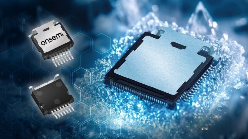
Onsemi has a T2PAK top-side cooled package for its EliteSiC MOSFETs. Image used courtesy of Onsemi
Why Is Packaging the Limiting Factor?
Silicon carbide has become the industry standard choice for high-voltage power stages, but the package around it often decides how much of that capability actually shows up in the final design. Through-hole parts like TO-247 are good at moving heat into a heatsink, though the longer leads start to work against it once layouts get tight by adding stray inductance and switching loss. Surface-mount options such as D2PAK clean up the current paths and help with faster switching, but they send most of the heat straight into the PCB, which is rarely where designers want it.
In dense power stages, neither approach is ideal. Designers are left trading switching speed against temperature margin, while board layouts grow more complex as they try to manage both electrical and thermal constraints at the same time.
What Does T2PAK Change?
T2PAK is a top-side cooled surface-mount package, which means heat leaves the MOSFET through the top of the device directly into a heatsink or cold plate rather than through the board. That single change addresses the core thermal bottleneck while preserving the short electrical paths that SiC devices rely on for fast switching.
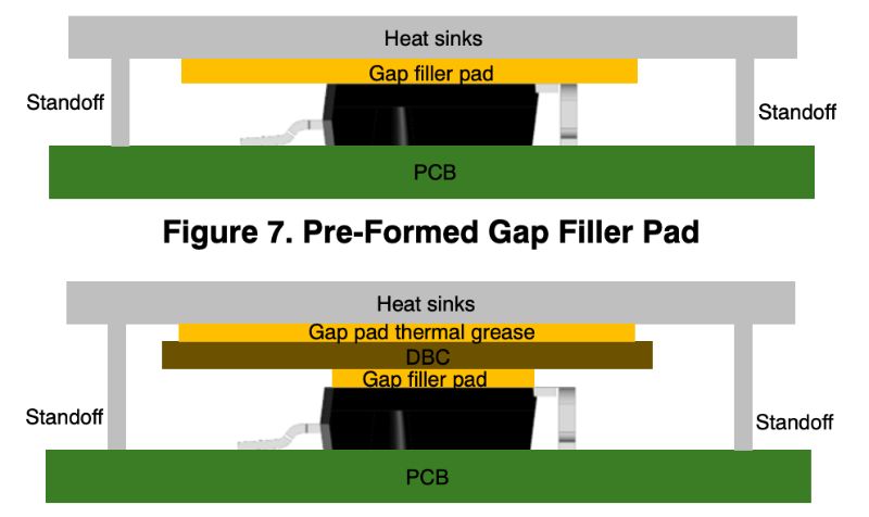
The design supports flexible thermal stacks using liquid gap fillers, pre-formed gap filler pads, and ceramic insulators. Image used courtesy of Onsemi
On the low-resistance end of the lineup, junction-to-case thermal resistance measures around 0.35°C/W, which is a slight improvement from most standard D2PAK packages. That improvement gives engineers more room to manage heat without reinforcing the board or adding copper.
Creepage clearances meet IEC 60664-1, and the package is designed to work with a range of thermal interface materials, whether the application calls for gap fillers or ceramic isolation.
Thermal and Electrical Benefits in Practice
Once heat is no longer pushed through the board, many of the usual side effects begin to disappear, as temperatures are able to stabilize, long-running systems behave more consistently, and efficiency holds up better as designs get tighter.
PCB constraints can eventually cap how much power can be handled, and beyond that point, gains come at the cost of layout complexity rather than improved switching. By routing heat directly into the cooling hardware, it keeps those limits from dominating the design.
What Applications Do These MOSFETs Support?
Applications that already separate electrical layout from thermal management stand to gain the most. In EV systems, power stages are commonly mounted against liquid-cooled structures. This tends to make it easier to pull heat away from the devices themselves. Industrial energy equipment also follows a similar pattern, such as in solar and storage systems that operate continuously and need stable efficiency over long service intervals.
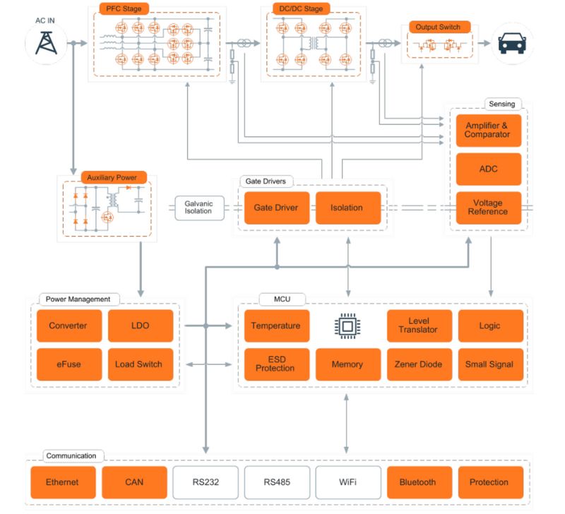
Typical block diagram for DC EV charging system. Image used courtesy of Onsemi
Data centers are also another emerging area, as liquid cooling spreads through power shelves and rack-level converters, top-side cooled MOSFETs integrate naturally with cold-plate architectures, helping manage heat from high-current AC-DC and DC-DC stages that support AI workloads.
With EliteSiC MOSFETs in the T2PAK package, Onsemi is addressing a practical problem that has limited how far SiC designs can be pushed. By rerouting heat away from the PCB and into the system’s cooling hardware, the package removes a long-standing compromise between thermal and electrical performance. For designers working on high-voltage, high-power systems, T2PAK is less about a new form factor and more about unlocking headroom that was already in the silicon.