Facebook
 Google
 GitHub
 Linkedin
The Impact of Direct Liquid Cooled Power Semiconductors
Eliminating insulation in power electronics could offer higher power density and efficiency without compromising reliability.
This article is published by EEPower as part of an exclusive digital content partnership with Bodo’s Power Systems.
The challenge in power electronics is to achieve higher power throughput in smaller devices at a reduced cost. These often contradicting targets lead to compromises. Higher currents lead to higher thermal stress in a given device, reducing its lifetime. Solutions with lower losses can be considered to counteract this, like replacing IGBTs with SiC-MOSFETs. However, the solution becomes more expensive. Another method is improved cooling. However, insulating substrates put physical limits on thermal transfer. The workaround? Drop the insulation requirement.
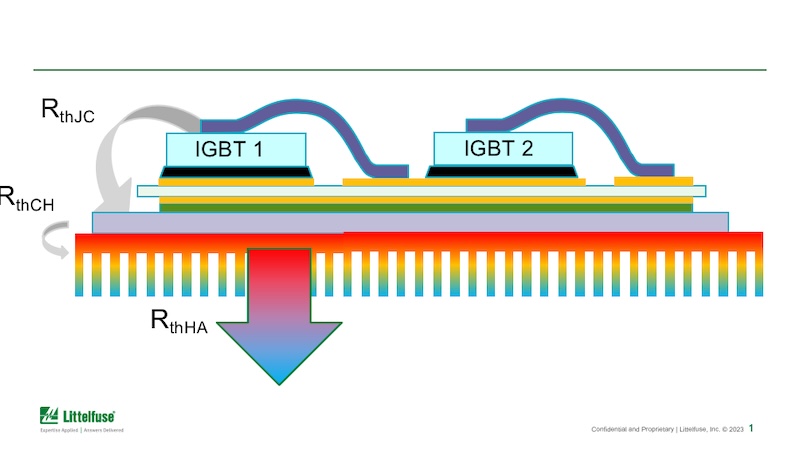
Figure 1. Structure of an insulated power semiconductor setup. Image used courtesy of Bodo’s Power Systems [PDF]
A Comparison of Semiconductor Modules
The most common semiconductor modules feature direct copper-bonded substrates (DCB) with insulating ceramic layers. A setup like this can carry multiple dies, as structuring the upper copper layer allows handling different potentials. Figure 1 schematically depicts such an approach.
In contrast, high-power disc devices are often combined with electrically active cold plates, as shown in Figure 2. The dominating thermal resistance within a setup shown in Figure 1 is provided by the ceramic layer. High-performance ceramics like aluminum nitride (AlN) feature up to 180 W/(mK) thermal conductivity. Still, the thickness needed to achieve the necessary isolation results in a large thermal resistance. The setup in Figure 2 improves the thermal performance as no electrical insulation between the power semiconductor and the heat sink is involved. Consequently, an electrically non-conductive cooling liquid like a de-ionized water/glycol mixture must be used, and its insulating quality must be monitored and maintained.
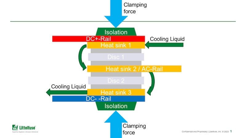
Figure 2. Power semiconductor arrangement with electrically active cold plates. Image used courtesy of Bodo’s Power Systems [PDF]
Eliminating Thermal Resistance
To eliminate the dominating thermal resistance of the DCB, an approach was followed, soldering the IGBT-dies directly to a suitable liquid cold plate of 40 x 80 mm². This way, the cold plate becomes the electric connection to the IIGBT’scollectors. DCB substrates are used to mount the power terminal at the emitter side as well as the control terminals. A test vehicle based on a different assembly technology was built to overcome the limitations inflicted by the bond wires. Here, a different die with a solderable front-side metallization was used. The bond wires were replaced using interconnecting clips soldered to the IGBT’s front side. As the clips cannot be soldered to the die directly, an interfacing pad is first soldered to the IGBT. The resulting test vehicle is pictured in Figure 3.
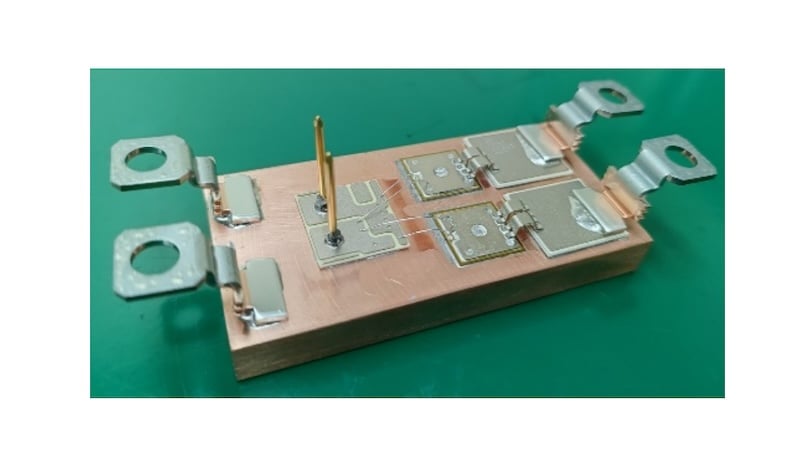
Figure 3. Clip-soldered test vehicle. Image used courtesy of Bodo’s Power Systems [PDF]
An IR-Camera-based measurement was conducted, and the result was 200 A per die, as seen in Figure 4.
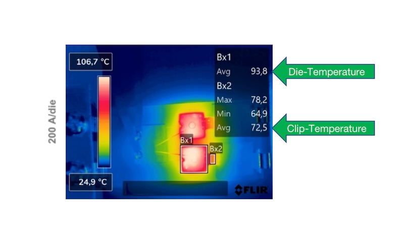
Figure 4. Thermographic measurement with clip-soldered material. Image used courtesy of Bodo’s Power Systems [PDF]
Any limitations imposed by using bond wires have been removed. The clip’s temperature remains well below 100°C at current densities that are beyond the capabilities of bond wires the die could carry.
A standard die with a current rating of 150 A was used for the study. Today’s industrial boundary conditions include a maximum inlet temperature of 65°C and a maximum chip temperature of 175°C. The measurements lead to a maximum power loss density of 380 W/cm² that can be dissipated from the chip by the setup. Notably, the die rated 150 A was well within its thermal limits while handling 200 A. For the targeted thermal conditions and 65°C inlet temperature, the maximum junction temperature of Tvj=175°C is reached at 250 A.
Electric Testing
Though the study focused on thermal performance, basic electrical behavior was also tested. The result from a double-pulse test is summarized in Figure 5.
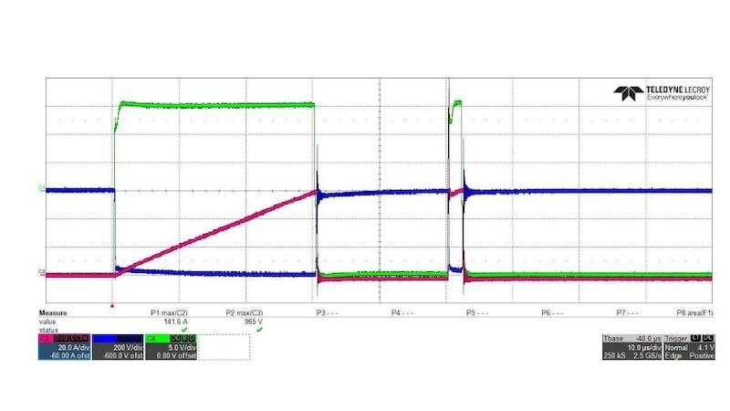
Figure 5. Results from the dynamic testing in double-pulse test equipment. Image used courtesy of Bodo’s Power Systems [PDF]
The tests revealed sufficiently clean switching, but due to the nature of the test setup, no further details were investigated. Though the layout of the devices studied was not optimized for switching, and a perfect switching behavior was not expected, the results were still good enough to be later transferred into potential series development.
Cyclic Load Testing
The outstanding thermal performance is a key factor in increasing the lifetime of a power electronic component. From the second design, several devices were subjected to a power cycling test (PCsec) as defined in IEC 60749.
The expectation was that the pad-and-clip assembly would achieve a higher lifetime than a system using bond wires as the failure mechanisms of bond-lift-off and bond-heel-crack are eliminated. However, as the pad is soldered to the chip’s front side, delamination of this interface is expected to happen eventually. The test was conducted with an inlet temperature of 12°C. In a cycle of 4 seconds with a 50% duty cycle, the chip temperature swing observed was 90 K with a load current of 250 A. Figure 6 reveals the outstanding thermal performance and low heat spreading within the cold plate.
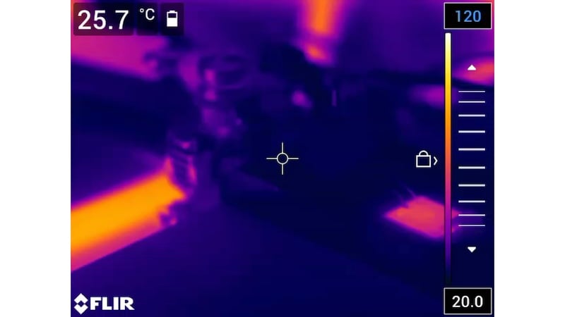
Figure 6. Thermal image of the chip during PCsec-Test. Image used courtesy of Bodo’s Power Systems [PDF]
The results from a long-term test are depicted in the graph in Figure 7.
It remains to be noted that the IGBT in this test had a rated chip current of only 150 A. So, despite staying within the given thermal limits for chip temperature, the chip operated well beyond the parameters used in a real-world application.
The end-of-life criteria for this test is an increase of the forward voltage of 5%. This value was reached after roughly 145.000 cycles. Classical solder bond technology reaches about 80.000 cycles under these conditions. As further potential for improvement is seen in the chip metallization, solder alloys, and solder processes, achieving at least twice the power-cycling capability compared to solder-bond devices does seem reasonable.
Potential Applications and Resulting Benefits
The structure chosen and the power density achieved make it obvious that such a design is meant for a high-power application. Applications that already feature liquid cooling and demand high power throughput can especially benefit from an insulated power semi-conductor arrangement.
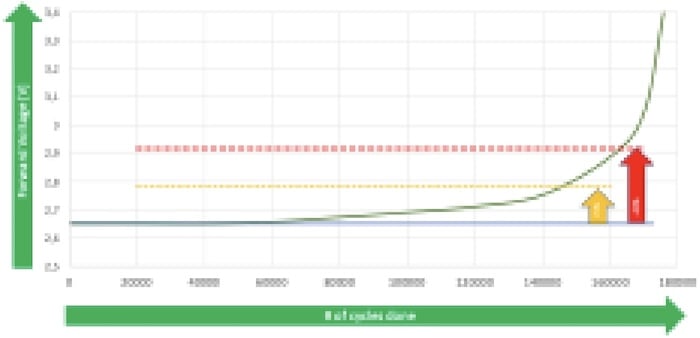
Figure 7. Results from the PCsec testing. Image used courtesy of Bodo’s Power Systems [PDF]
Such an approach targets renewable energy generation in windmills or metal welding by induction heating. With the heat sink forming the connection to the IGBT’s collector, the scheme is a good choice for building single switches with high current-carrying capabilities, as schematically drawn in Figure 8.
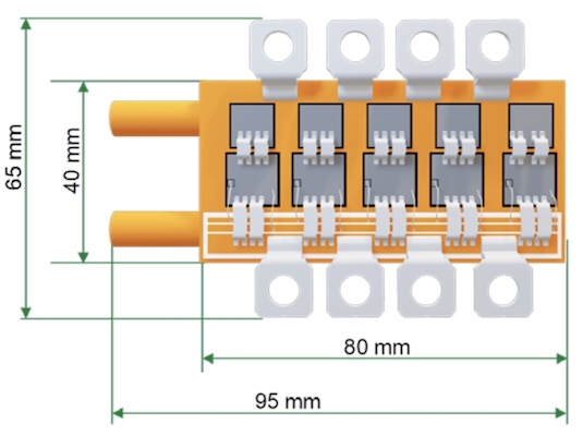
Figure 8. 1200 A-Device in non-isolated setup. Image used courtesy of Bodo’s Power Systems [PDF]
This version, equipped with a 250 A chipset, resembles a 1200 A single switch with an envelope of 123.5 cm³.
A half-bridge consisting of two such devices consumes about 250 cm³ of space. In comparison, high-power modules used today demand up to 700 cm³.
A further benefit of integrated liquid cooling is that the necessary surrounding housing is no longer burdened with the high temperatures commonly seen in power semiconductors. This opens a path to using lower-grade plastics, potentially even materials that are easy to recycle, which will be a major topic in the years ahead.
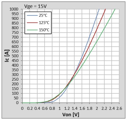
Figure 9. IC vs. VCE of a newly designed IGBT with high desaturation limits. Image used courtesy of Bodo’s Power Systems [PDF]
As for the use of resources, a half-bridge built from the device in Figure 8 has a mass below 0.7 kg, which is less than half the weight of current designs.
Sacrificing a fraction of the performance by replacing the copper heat sink with aluminum would allow for both cost and weight reduction.
Highly efficient cooling is also the key to fully exploiting the capabilities of IGBTs with very high desaturation limits. The limiting triangle of forward voltage, switching performance, and short-circuit robustness spans the optimization area for IGBT technology. Chips with low switching losses tend to have higher forward voltage and vice versa, as long as the short-circuit capability remains untouched. The diagram in Figure 9 reflects the forward voltage of an IGBT optimized for low forward voltage.
This 1200 V-chip is rated 200 A and generates 240 W of losses at this point of operation. Though the chip could easily withstand currents up to 450 A, the losses grow to 720 W or, in this case, 360 W/cm².
Such power loss densities in assemblies with ceramic isolation materials would lead to chip temperatures that are too high, even when high-performance ceramics are installed.
With the direct liquid cooling approach, up to 380 W/cm² has been achieved, making it possible to operate the chip at this point without exceeding its thermal limits.
Thus, the device in Figure 8 could carry more than 2 kA of current, potentially reaching the tolerable current density limits within the terminals used.
Pushing the Limits of Power Density in Power Semiconductors
Due to isolation requirements, increasing power density in today’s power semiconductors has physical limits. To push these limits, new methods to extract heat from power semiconductors more efficiently must be identified. One way is direct liquid cooling combined with a suitable chip and interconnection technology. The shift from classical isolated assemblies to non-isolated counterparts opens the door to increasing power density by a factor of ten compared to today’s options.
This is not limited to IGBT technology but can be transferred to wide-band-gap semiconductors in the very same way.
This article originally appeared in Bodo’s Power Systems [PDF] magazine.
Related Content