Facebook
 Google
 GitHub
 Linkedin
Game Changers in SiC Power Device Performance and Reliability
SiC technology is crucial in driving the transition toward electric mobility and enhancing the efficiency of renewable energy systems. Despite significant enhancements in the quality and availability of 4H-SiC material, the challenge of producing low defect density and high-performance SiC wafers for optimal yields still persists.
This article is published by EEPower as part of an exclusive digital content partnership with Bodo’s Power Systems.
Since the introduction of the first commercial single-crystal SiC wafers in the early 1990s, no change has been made to their composition, only changing their diameter and reducing their defectivity over time. SmartSiC is an engineered substrate based on a new paradigm, combining on a single substrate a high-quality top layer made of single-crystal SiC bonded over a highly-electrically conductive polycrystalline SiC handle wafer to allow for unprecedented gains in terms of device performance and reliability.
Silicon Carbide (SiC) technology in power electronics is crucial in driving the transition toward electric mobility and enhancing the efficiency of renewable energy systems. With the increasing demand in the market, power semiconductor companies are under pressure to rapidly scale up their production capacity. Despite significant enhancements in the quality and availability of 4H-SiC material, the challenge of producing low defect density and high-performance SiC wafers for optimal yields still persists.
In response to this pressing need, a groundbreaking SiC-engineered substrate has been introduced to address the industry’s requirements. The unveiling of a dedicated manufacturing line in September 2023 marks a significant milestone, signaling the start of high-volume manufacturing for this innovative SiC substrate. This strategic initiative is poised to revolutionize the landscape of SiC technology, offering a breakthrough solution to the current manufacturing constraints and paving the way for enhanced efficiency and performance in power electronics applications.
The fabrication of the SmartSiC substrates relies on the Smart Cut technology and offers significant advantages in the fabrication of SiC devices. Here’s a breakdown of its key features and benefits:
- High-Quality SiC Top Layer: The Smart Cut technology facilitates the transfer of a high-quality SiC layer on top of a handle wafer, serving as a seed for the drift epitaxy to be grown. This process is crucial for optimizing device yield and reliability, ensuring that the resulting devices meet stringent quality standards.
- Low Resistivity Handle Wafer: The technology incorporates a low-resistivity handle wafer with a typical resistivity of 2 mOhm.cm (standard SiC material resistivity is around 20 mOhm.cm). This feature enhances device conduction while also enabling the minimization of switching losses, ultimately improving the overall performance of applications based on SiC devices.
- Compatibility with Different Wafer Diameters: The Smart Cut technology is compatible with any substrate diameter and used for 150 mm and 200 mm wafers.
Based on the characteristics described above, the obtained SmartSiC Engineered Substrate consists of a sub-micron-thick (between 400 and 800 nm) high-quality, single-crystal 4H-SiC top layer bonded on top of a polycrystalline SiC handle wafer. The final engineered substrate has a thickness of 350 µm for 150 mm wafers and 500 µm for 200 mm wafers. This composition ensures the structural integrity and performance of the substrate, contributing to the reliability and efficiency of SiC devices.
Additionally, by enabling the reusability of initial single crystal donor wafers due to the low thickness of the top single crystal layer, the SmartSiC technology offers the most efficient use of hard-to-achieve SiC boules. Compared to conventional wafering processing of SiC material, which typically allows the extraction of a maximum of 50 wafers per boule, the Smart Cut technology allows for the preparation of up to 500 engineered substrates from the same boule. This substantial increase in productivity represents a significant cost-saving and resource-efficient solution for SiC device fabrication.
The Smart Cut process applied to the manufacturing of SmartSiC-engineered substrates is shown in Figure 1.
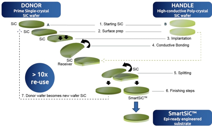
Figure 1. Smart Cut technology adapted to silicon carbide. Image used courtesy of Bodo’s Power Systems [PDF]
To investigate the advantages of SmartSiC engineered substrates versus standard single-crystal 4H-SiC wafers, n-type, 13 mOhm/650 V Gen2 planar SiC MOSFETs were manufactured on both types of substrates and processed simultaneously as a single batch.
The single-crystal, 4H-SiC wafer, considered as the reference, is Nitrogen-doped with a typical resistivity of 20 mOhm.cm, whereas the poly-SiC handle wafer of the SmartSiC substrate has a higher Nitrogen-doping and a typical resistivity of 2mOhm.cm. The drift epitaxy is Nitrogen-doped, with a doping concentration ND≈2x1016cm-3. Phosphorus and aluminum implantations were used to form, respectively, source and body regions. The gate oxide was a 55nm thick SiO2 layer, while highly doped n-type poly-Si was used as a gate electrode. The structures of the test vehicle MOSFET on the standard single-crystal SiC wafer and on the SmartSiC™ substrate are shown in Figure 2.
Results
The results obtained on the 13 mOhm 650 V Gen2 planar SiC MOSFETs are presented here.
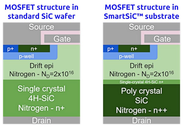
Figure 2. Structure of the Gen 2 planar SiC MOSFET used as test vehicle as implemented on single-crystal 4H-SiC wafer (left) and on SmartSiC substrate (right). Image used courtesy of Bodo’s Power Systems [PDF]
Figure 3 presents a comparison of the device’s RDSon. Results show an average reduction of the on-resistance of around 24% favorable to the SmartSiC substrates. This improvement is due to the much lower resistivity of the poly-SiC handle wafer of SmartSiC substrates, as well as its capacity to make much lower resistivity metal contacts (back-side drain contact in this case).
Such a strong reduction of RDSon (~24%) is close to what can be expected during the transition from one device generation to the next.
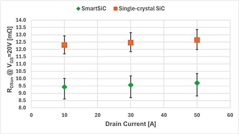
Figure 3. Ron comparison for a 13 mOhm/650 V Gen2 SiC MOSFET manufactured in single-crystal SiC and SmartSiC substrates. Image used courtesy of Bodo’s Power Systems [PDF]
Figures 4 and 5 present threshold voltage and drain leakage current for the same device manufactured in a single-crystal SiC wafer and SmartSiC substrate, respectively. The results show equivalent behavior for these parameters for both types of substrates.
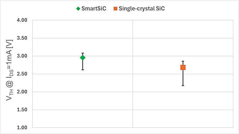
Figure 4. Vth comparison for a 13 mOhm /650 V Gen2 SiC MOSFET manufactured in single-crystal SiC and SmartSiC substrates. Image used courtesy of Bodo’s Power Systems [PDF]
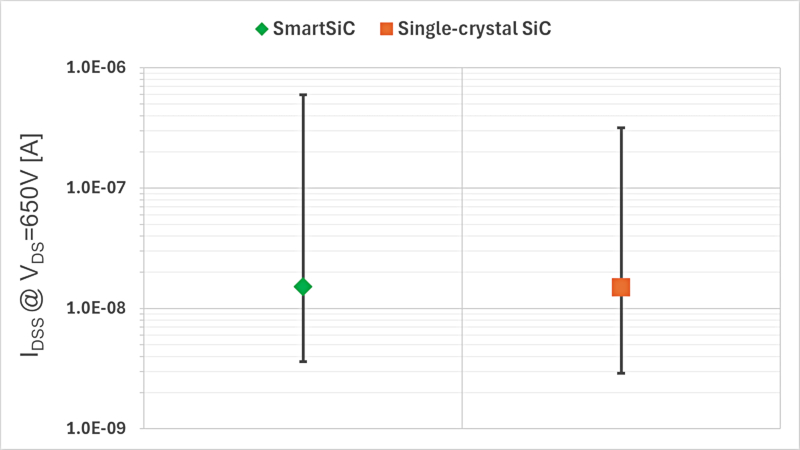
Figure 5. IDSS comparison for a 13mOhm / 650V Gen2 SiC MOSFET manufactured in single-crystal SiC and SmartSiC™ substrates. Image used courtesy of Bodo’s Power Systems [PDF]
Potential for Other Devices
As shown in the previous sections, in contrast to standard single-crystal SiC substrates with an electrical resistivity of around 20 mOhm.cm, polycrystalline SiC material can achieve resistivity levels as low as 1 mOhm.cm, with a typical value around 2 mOhm. cm. Additionally, the high doping level of polycrystalline SiC contributes to lowering the contact resistance well below 10 µOhm.cm². These characteristics enable SmartSiC substrates to increase the device’s current density, thus allowing the reduction of the device die size for both MOSFETs and diodes.
In particular, for FETs, although the total gain is dependent on the initial device-specific resistance (Ron.A) and die thickness, Figure 6 shows that the more advanced the FET technology, the higher the gain obtained. By initial Ron.A we mean that of the device when manufactured on a single-crystal SiC wafer. As an example, for a FET with an initial Ron.A of 2.8 mOhm.cm² and a die thickness of 180µm, figure 5 shows that when manufactured on SmartSiC substrates, the new Ron.A is 15% lower (a gain of 15%). Notice that this gain is independent of the device’s voltage rating.
The value of 2.8 mOhm.cm² taken in the previous paragraph corresponds to the current state-of-the-art case of a 1200 V SiC MOSFETs. However, when looking at the device generations to come in the next years, Ron.A gains (reductions) in excess 20% can be expected, always presenting the advantage of “at least” one additional generation when using SmartSiC-engineered substrates.
An extreme gain case takes place today with state-of-the-art JFETs, the preferred choice for 400 V and 800 V solid-state circuit breakers for electric vehicles. Taking as an example a 750 V SiC JFET with an initial Ron.A of around 0.7 mOhm.cm², gains of around 30% can be expected.
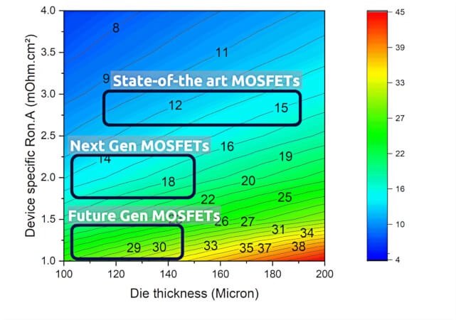
Figure 6. Ron.A reduction enabled by SmartSiC used for 1200 V SiC MOSFETs as a function of the initial Ron.A and die thickness. Image used courtesy of Bodo’s Power Systems [PDF]
Last but not least, SmartSiC-engineered substrates show, at first analysis, to be further confirmed with specific electrical evaluation, a valuable ruggedness against bipolar degradation. This degradation phenomenon appears on SiC substrates due to the gliding (extension) of basal plane dislocations (BPD) within the SiC crystal when exposed to high levels of bipolar current (due to electrons and holes simultaneously). This takes place generally during the reverse conduction of SiC MOSFETs when current goes through the PiN-type body diode of the transistor.
To validate such ruggedness, epitaxial standard single-crystal SiC wafers, as well as SmartSiC substrates, were exposed to stress conditions aimed at revealing bipolar degradation. this was carried out by using the E-V-C technique developed by ITES, Co. After stress, it appears that both the number of Shockley staking faults, the indicator that bipolar degradation takes place, and their typical size are lower in the case of SmartSiC compared to the results obtained in standard SiC wafers. The results suggest that the SmartSiC design possesses an inherent ruggedness advantage against bipolar degradation over single-crystal wafers. This characteristic was previously evaluated through a forward-current stress test conducted on a 4H-SiC epitaxial layer subjected to proton irradiation.
Future Generations
Under the current context of accelerating the deployment of SiC devices for the decarbonization of the mobility and power conversion industry, SmartSiC offers unmatched characteristics, allowing for higher power density and more reliable applications.
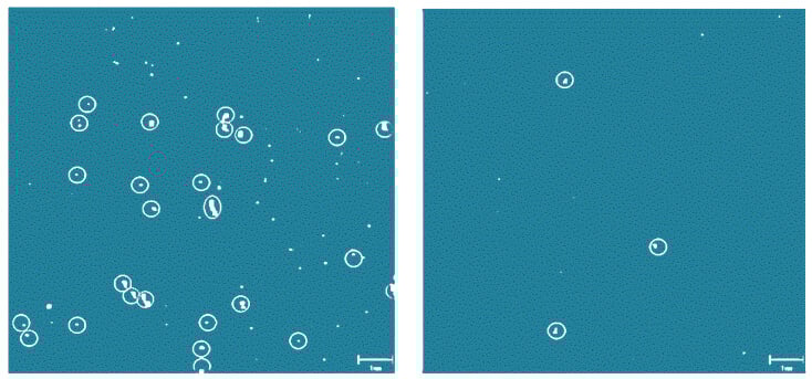
Figure 7. Typical 10x10 mm observation fields post UV illumination (here 150 W) 420 nm BPF PL of bipolar degradation severity between bulk+epi (left) vs. SmartSiC+epi (right). Image used courtesy of Bodo’s Power Systems [PDF]
Results obtained from MOSFETs made on single-crystal SiC wafers and SmartSiC substrates show that the latter offer gains equivalent to those obtained when moving from one device generation to the next.
The gains validated on currently available device generations show that the advantages of SmartSiC would still be more noticeable in future device generations, as well as in other devices with much lower Ron.A, such as JFETs.
The work necessary to obtain the results presented was carried out within the TRANSFORM project (funded by the Key Digital Technologies Joint Undertaking under Grant Agreement No. 101007237).
This article originally appeared in Bodo’s Power Systems [PDF] magazine and is co-authored by G. Picun, WBG Business Development Manager, SOITEC; Dr. L. Zumbo, R&D Staff Engineer, STMicroelectronics; Dr. E. Guiot, WBG Product Design Manager, SOITEC; G. Bellocchi, R&D Staff Engineer, STMicroelectronics; A. Guarnera, SiC Power Devices Design Group Manager, STMicroelectronics; S. Rascunà, Advanced Research Senior Manager; A. Imbruglia, Funded Projects Advanced Design Program Manager & Expert, STMicroelectronics; G. Arena, Sr. Director of R&D Technology Development, STMicroelectronics; M. Saggio, R&D Design Director, STMicroelectronics.