Facebook
 Google
 GitHub
 Linkedin
Using Fast Recovery Diode MOSFETs in Power Supplies
This article outlines the issues engineers must consider when designing Super Junction-based power devices.
This article is published by EEPower as part of an exclusive digital content partnership with Bodo’s Power Systems.
“Super Junction” technology has dominated the power MOSFET market where breakdown voltage exceeds 600 V due to its superior figure-of-merit. There are certain considerations engineers must make when designing Super Junction-based power devices to enhance efficiency, power density, and reliability in power supply applications.

Image used courtesy of Adobe Stock
Engineering Considerations
As shown in Figure 1, one of the first considerations is that the P columns extend from the base region to create a “charge balance” in the drift area for higher doping concentration, namely lower resistance in the corresponding region. The extended junction area leads to a drawback of excessive reverse recovery charge.
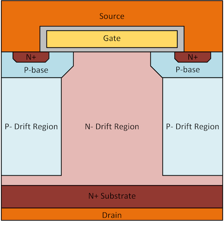
Figure 1. P-N junctions in Super Junction MOSFETs. Image used courtesy of Bodo’s Power Systems [PDF]
Figure 2 shows a typical half-bridge configuration in which the current freewheels through the body diode of the high-side MOSFET during the dead time before the low-side MOSFET turns on. The body diode reverse recovery happens when the low-side MOSFET starts to turn on. The low-side MOSFET sees a negative current spike due to the reverse recovery charge of the high-side MOSFET. This causes an excessive turn-on loss in the low-side MOSFET. At the same time, the high-side MOSFET sees a high slew rate voltage rise and a spike voltage during the Tb period, which can cause an overstress on the device.
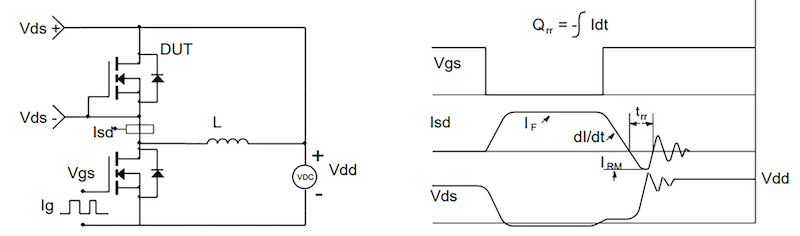
Figure 2. Body diode reverse recovery in half-bridge circuit. Image used courtesy of Bodo’s Power Systems [PDF]
Ultimately, as shown in an example in Figure 3, a 600 V Super Junction device failure is caused by the body diode recovery when the forward current and the current slew rate are beyond the device’s safe operation limit.
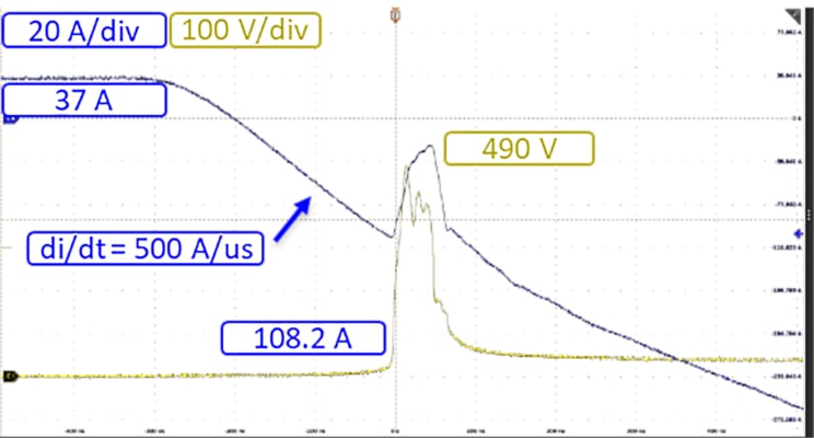
Image used courtesy of Bodo’s Power Systems [PDF]
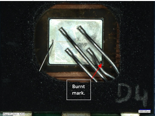
Figure 3. Illustrates a device failure caused by the body diode reverse recovery. Image used courtesy of Bodo’s Power Systems [PDF]
An issue to be aware of is that body diode reverse recovery in Super Junction-based power devices has deeply impacted the selection of high-voltage power devices for power supply designs. Figure 4 shows a typical circuit in AC/DC power supply. In the power factor correction stage, SiC Schottky diode instead of a synchronous rectifier FET is used as the high-side device because the switching loss caused by the reverse recovery of a synchronous rectifier is too high with the target switching frequency (usually above 50 kHz).
In the DC-DC stage, the soft-switching LLC circuit is used where hard commutation of the high-voltage devices does not happen in normal operation mode. The device’s hard commutation causes the body diode to reverse recovery; thus, it will not be seen in this case. However, hard commutation can happen in the LLC circuit during abnormal operation conditions such as start-up and short-circuit transients. Protections against such transients are normally required in the controller design of the LLC circuit. Failure to prevent the hard commutation in the LLC circuit could lead to a failure in the high-voltage devices due to the very snappy body diode reverse recovery transient.
There are circumstances where the high-voltage device body diode reverse recovery can’t be avoided. For example, cycle-by-cycle hard commutation protection is not available in high-power LLC converters with digital controllers. In high-voltage motor drive applications, active devices (MOSFET/IGBT) are needed for both high- and low-side switches. Improved body diode performance regarding the reverse recovery charge and reliability is a key requirement for the high-voltage power device in these applications.
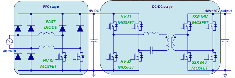
Figure 4. Typical AC/DC power supply circuit structure. Image used courtesy of Bodo’s Power Systems [PDF]
αMOS5 Fast Recovery Diode Technology
The αMOS5 Fast Recovery Diode (FRD) MOSFET platform developed by Alpha and Omega Semiconductor (AOS) is specifically optimized for low reverse recovery charge and switching robustness. Electron irradiation is applied in this technology to control the lifetime of the bipolar carriers during the reverse recovery phase. It creates defects to serve as recombination centers and accelerates the process of electron/hole pair recombination of the FRD during the forward biasing and the reverse recovery stage, significantly reducing the total number of excessive charges stored in the FRD drift region.
Comparing the Qrr waveforms of the same Super Junction structures, but with different carrier lifetime control, the ER-processed part shows a significant reduction in Qrr value. Suppressed Qrr means that a smaller power spike level will surge through the FRD, thus suppressing the risk of thermal failure.
It is important to note that the MOSFET active/termination transition region is the most vulnerable to reverse recovery failure as it passes high current density with its limited area size. A key benefit of the αMOS5 platform is that it employs a conservative termination design to evenly spread the electric field across the transition region. This optimization prevents localized hot spot burnout due to excessive power density during the reverse recovery tb phase.
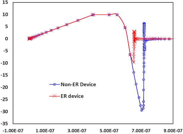
Figure 5. ER Controlled reverse recovery waveform. Image used courtesy of Bodo’s Power Systems [PDF]
Test Results
The safe operation condition regarding the body diode reverse recovery is validated with AOS αMOS5 FRD MOSFET tests. The test result is provided in the device datasheet. Figure 6 shows the test waveform of AOS’ AOK042A60FD 600 V 42 mΩ αMOS5 SJ MOSFET and two competitors with similar BVdss and Rdson specifications. The test was conducted with 50 A forward current and 1000 A/us slew rate at three different temperatures. As shown in Table 1, the AOK042A60FD passed the test at 200°C, while the competitors failed the test even at lower temperatures.
It is worth noting that AOK042A60FD shows the lowest drain voltage slew rate in the Tb period waveform. This helps the device survive the harsh reverse recovery transient and improve its EMI performance. The test result shows that the AOS αMOS5 FRD SJ device provides highly effective body diode robustness in the reverse recovery transient, which is crucial in bridge-type applications such as LLC converters to ensure the highest system reliability in abnormal and transient conditions.
Table 1. Body diode reverse recovery robustness test result for AOK042A60FD
| DUT | IF (A) | di/dt (A/us) | dv/dt (ns) | ||||
| 50 | 1000 | 25°C | 150°C | 200°C | |||
| AOK042A60FD | 104 (pass) | 46 (pass) | 38 (pass) | ||||
| Competitor 1 | 160 (pass) | 92 (pass) | 74 (fail) | ||||
| Competitor 2 | 134 (pass) | 122 (fail) | |||||
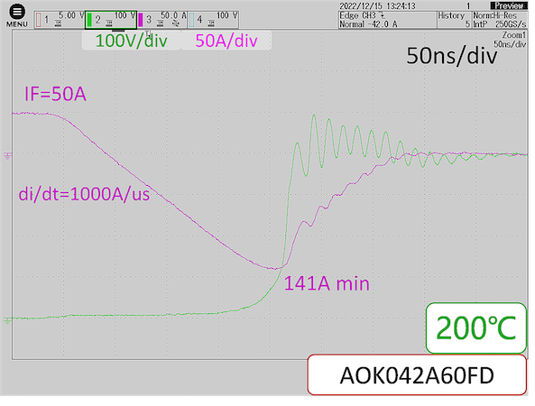
Image used courtesy of Bodo’s Power Systems [PDF]
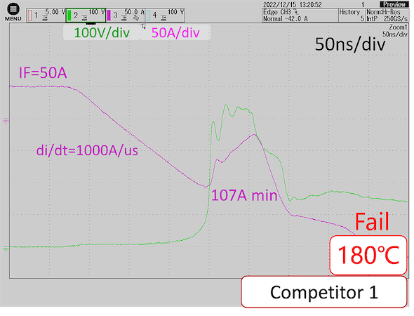
Image used courtesy of Bodo’s Power Systems [PDF]
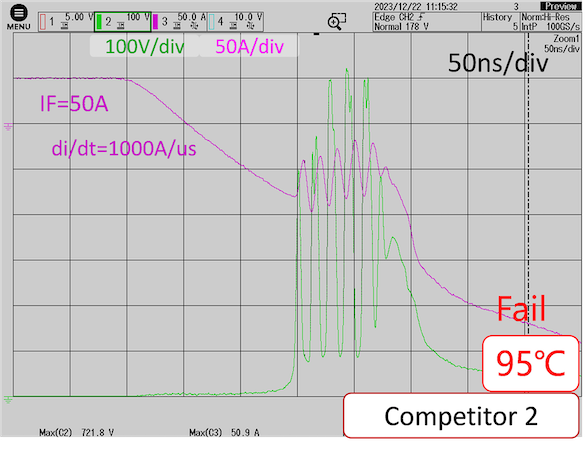
Figure 6. Body diode reverse recovery test performed on two competitive products and the AOK042A60FD αMOS5 FRD MOSFET (VDD = 400 V, IF = 50 A, di/dt = 1000 A/us). Image used courtesy of Bodo’s Power Systems [PDF]
This article originally appeared in Bodo’s Power Systems [PDF] magazine and is co-authored by Ziwei Yu, Application Manager; Jorge Ramos, Sr. Application Engineer; Wendi Wang, Staff Engineer; and Richard Zhang, Sr. Director of MOSFETs, with Alpha and Omega Semiconductor.