Facebook
 Google
 GitHub
 Linkedin
Unlocking the Potential of SiC MOSFETs With Front-Side Copper Metallization
Learn how front-side copper metallization (FSM) is unlocking the full potential of Silicon Carbide (SiC) MOSFETs, especially as devices shrink in size to improve performance.
Article co-authored by Sanan Semiconductor’s Dr. Tzu Kun Ku, Chief Process Officer, and Dr. Wesley Chih-Wei Hsu, Head of Research and Development.
This article is published by EEPower as part of an exclusive digital content partnership with Bodo’s Power Systems.
In this article, we explore how front-side copper metallization (FSM) is unlocking the full potential of Silicon Carbide (SiC) MOSFETs, particularly as devices shrink in size to boost performance. Copper, with its superior electrical, thermal, and mechanical properties, offers significant advantages including higher reliability, better heat dissipation, and support for advanced packaging, such as double-sided cooling.
Efficiency and power density requirements for power electronic systems continue to increase. As a consequence, the Rdson*Area figure of merit (FOM) of Silicon Carbide (SiC) Mosfets is continuously improving, primarily driven by the shrinking of the MOS channel (pitch). This reduced channel resistance naturally enables higher nominal currents per unit die area (under comparable boundary conditions). However this introduces two thermal challenges.
First: a smaller die also implies a higher thermal resistance (assuming the rest of the package remains the same). Second: Power dissipation (conduction) is directly proportional to the resistance, but to the square of the current, thereby resulting in higher power dissipation per unit area of the chip despite the reduced channel resistance. Both these challenges make it necessary to improve power sinking capabilities of the chip to reap the full benefits of FOM improvements.
Furthermore, heat generation in power semiconductors is usually localized on the upper surface (MOS head), resulting in higher localized temperatures on the Front-side (FS) (also sometimes called Top-side (TS)) than on the back side (BS). Furthermore, there are dynamic conditions, for example, short circuit where the frontside is heated significantly higher than the backside. As chip temperature directly impacts reliability, the FS metallization is crucial to the chip’s performance and must be paid special attention.
Advanced Module Packaging Necessitates Additional Copper Pads on the Chip Front Side
Aluminium-based front-side metallization (FSM) has been traditionally used in power semiconductor chips for cost optimization. During packaging, these chips are usually bonded on the FS with Aluminium bond wires. In the application, the current flowing through the bond wires is usually cycled, firstly due to switching during the duty cycles, and secondly due to variations in the load itself. This causes continous expansion and contraction of the bond wires, resulting in fatigue, and eventually leading to plastic deformation and failure.
The further the melting point of the bond wire from the operating temperature, the lower will be the fatigue, and lower the failure rate. As the maximum allowed junction temperatures of power semiconductors continue to increase, it is imperative that interconnects with higher melting points would be explored, to reach the same, if not higher, levels of reliability. This is where Copper presents itself as a promising alternative.
| Parameter | Aluminium | Copper |
| Resistivity [1e-9 Ω·m] | 23.5 | 16.7 |
| Melting Point [°C] | 660 | 1080 |
| Thermal Conductivity [W/m·K] | 220 | 400 |
| Co-efficient of Thermal Expansion [1e-6 /K] | 25 | 17 |
| Yield Strength [MPa] | 30 | 70 |
Table 1. Comparison of key parameters of Aluminium and Copper.
As can be seen from the above table, Copper has a significantly higher melting point compared to Aluminium, which makes it more stable with respect to temperature. Also, Copper has a lower resistivity, resulting in lower ohmic losses in the bond wires, enabling a higher current capability for the same cross section.
Furthermore, Copper has a higher thermal conductivity compared to Aluminium, resulting in a better heat extraction from the die. Mechanically, Copper is stronger compared to Aluminium, as is also evident from its higher yield strength. All these factors, make Copper bond wires a better alternative to Aluminum.
(a)
(b)
(c)
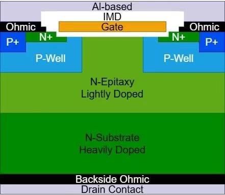
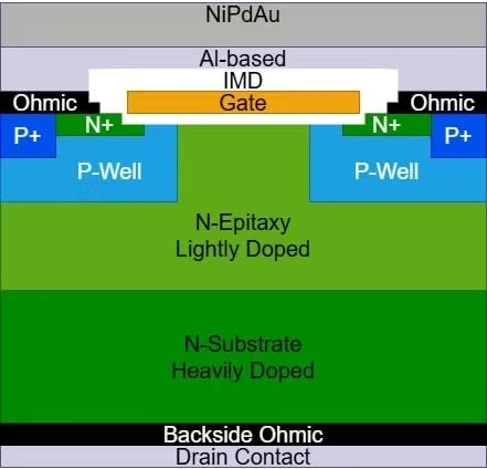
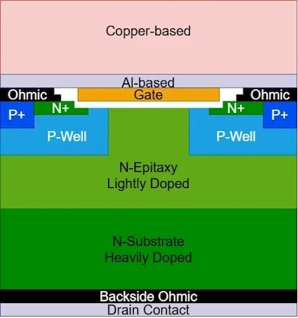
Figure 1. Representative Unit cell of the (a) Automotive Qualified SiC Planar Mosfet Technology with Aluminium-based FSM currently in Mass Production, (b) option with an additional NiPdAu Pad (c) Automotive SiC Planar Mosfet with Copper Metallization, currently in development (Images not to scale). Image used courtesy of Bodo’s Power Systems [PDF]
To support the higher forces and higher ultrasonic energies during the bonding of Copper wires and also the higher stresses in the application, the FSM of the chip must be suitably equipped. This implies that standard Aluminium-based FSM alone would not work, and an additional thicker copper-based metallization would be preferable. This has lead to an increasing adoption of Front-side Copper metallization.
Sanan’s Current SiC MOSFET Offering
Sanan has already released the Gen-1 SiC Mosfet based on the planar structure targeting industrial and automotive applications. Subsequently, cell engineering of the above planar structure has lead to significant improvements in the Rds*A Figure-of-Merit (FOM) which is available as Gen-2 (released) and Gen-3 (to be released later in 2025).
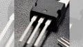
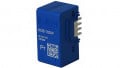
The current generations have an Al-based FSM (see Figure 1 (a)). Depending on the application, an additional layer of Ni/ Pd/Au can be offered (see Figure 1 (b)). Current portfolio extends from Rdson classes of 10mΩ - 1000 mΩ, in voltage classes 650V, 750V, 1200V, 1700V and 2000V, industrial and automotive qualified devices, available as bare dies, standard discrete packages such as TO-247, D2PAK, top-side cooled, and customer specific modules [2].
Furthermore, a trench structure (in early development), and a super-junction Mosfet (in early concept development) are expected to significantly enhance the FOM of the SiC mosfets, bringing them closer to Si devices in terms of cost-performance.
Sanan’s MOSFET Offering with Top Side Copper
To reap the full benefits of the SiC MOS FOM improvements, Sanan is also developing a SiC Mosfet technology with electroplated Copper-based FSM (see Figure 1 (c)). This is also shown in more detail in Figure 2.
Copper needs a barrier layer to avoid reaction with the SiC, polysilicon etc. For the electroplating process, a seed layer has to be first deposited. The electroplating process allows for a copper thickness of up to 20 µm as shown in the FSM stack in Figure 2.
Additionally, a PI (polyimide) layer plays the crucial role of protecting the chip surface, releasing mechanical stress, and enhancing surface planarity, which ultimately improves device reliability. This flexibility enables customers to select the optimal structure based on electrical performance, thermal needs, and cost constraints.
Key process features include:
- Electroplated copper layers ranging from 8 to 20 μm
- PI passivation to improve environmental resistance
With these capabilities, Sanan delivers flexible, high-reliability frontside Cu solutions that are well-suited for modern high-power and high-frequency applications, such as automotive traction inverters, renewables and power supplies.
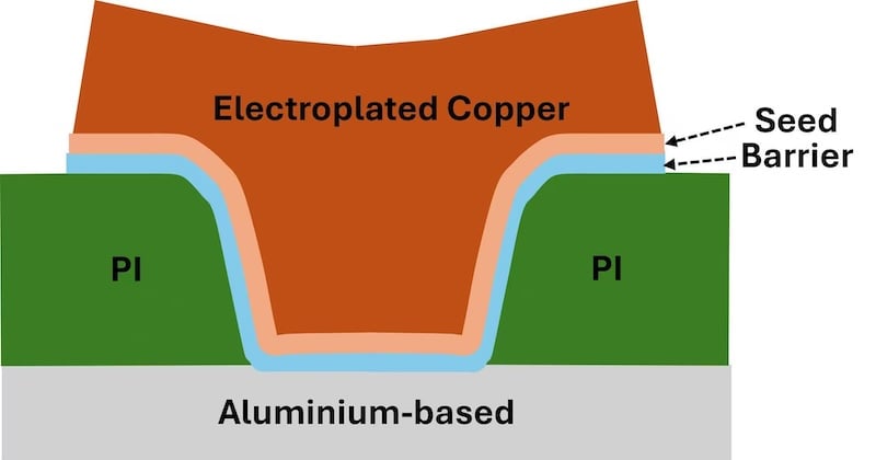
Figure 2. Sanan SiC Mosfet Copper-based Front side metallization stack (not to scale). Image used courtesy of Bodo’s Power Systems [PDF]
Advantages of Front-Side Copper Metallization
- Higher Junction temperature Operation: Copper, on account of its higher melting point compared to Aluminium, can allow the chip to operate at a higher temperature without any adverse impact on the reliability
- Higher Reliability for the same application conditions: On account of its lower resistivity, higher thermal conductivity, higher melting point and higher mechanical strength, copper FSM offers overall higher power cycling capability, resulting in a higher reliability for the same boundary conditions.
- Enabler of advanced packaging technologies: Copper FSM, owing to its superior strength, can allow for copper wire bonding which can significantly improve not only the current density, but also the power cycling capability.
- Enabler of double side cooled packages: Integrating Copper FSM in SiC MOSFETs can streamline the packaging process. The strong, solderable copper surface facilitates pressure contact or solder joints, eliminating the need for wire bonding altogether and going for copper clips or spacers, thereby further enhancing current density and power cycling reliability. This not only improves the parasitic behaviour, but also enables double sided cooling, which can drastically improve power density.
- Enhanced short circuit robustness and pulse current capability: Copper FSM can help to transport heat from the chip FS, which is usually the localized source for heat generation in SiC, thereby improving robustness under dynamic conditions such as short circuit, pulsed operation or even active short circuit.
- Higher power density: All the above mentioned aspects result in an overall higher power density while using Copper FSM, in comparison to Aluminium.
Thus, FS Copper helps to break through conventional limitations and unlock new levels of performance in power module design.
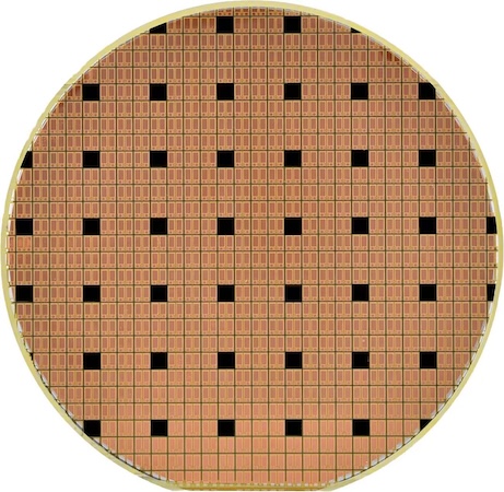
Figure 3. Sanan’s 750V SiC Mosfet wafer with front-side Copper Metallization (presented at PCIM Nuremberg May 2025). Image used courtesy of Bodo’s Power Systems [PDF]
References
[1] “Silicon Carbide Power Products”, Product Brief, Sanan Semiconductors
This article originally appeared in Bodo’s Power Systems [PDF] magazine and is co-authored by Dr. Wesley Chih-Wei Hsu, Head of Research and Development and Dr. Ajay Poonjal Pai, Director of Innovation, and Dr. Tzu Kun Ku, Chief Process Officer, Sanan Semiconductor.