Facebook
 Google
 GitHub
 Linkedin
WBG Meets Top-Side Cooling for Sustainable EV Power Conversion
Technologies like top-side cooling can help designers achieve high thermal performance and reduce assembly expenses in electric vehicles.
This article is published by EEPower as part of an exclusive digital content partnership with Bodo’s Power Systems.
The world of global mobility is on the cusp of a remarkable shift. In 2024, global EV sales are expected to soar by about 20 percent as governments and consumers try to mitigate the effects of climate change. By 2030, EVs are forecasted to account for at least two-thirds of global car sales.
With automakers striving to slash EV costs, efficient and sustainable power conversion systems are vital to meet the rising demands and power requirements. To that end, the adoption of wide-bandgap (WBG) semiconductors, such as silicon carbide (SiC) and gallium nitride (GaN), enables efficient, powerful, and long-term cost-effective power solutions. To build on that, innovative technologies like top-side cooling can help designers achieve optimal thermal performance and reduce assembly expenses.

Image used courtesy of Adobe Stock
Power Conversion Systems
The power conversion systems in EVs, particularly the onboard charger and DC-DC converters, are essential to managing the flow of electricity within the vehicle, optimizing the charging process, and facilitating the integration of various power sources. These power conversion systems are pivotal for the overall performance, efficiency, and user experience of EVs. Their proper functioning is essential to maximize the range, reliability, and functionality of electric cars, making them indispensable in the transition towards sustainable transportation.
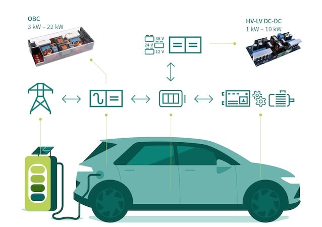
Figure 1. OBC and DC-DC power conversion systems in EVs. Image used courtesy of Bodo’s Power Systems [PDF]
Increasing power levels, bidirectional operation support (V2X), and faster adoption of 800 V battery systems have introduced new levels of complexity to OBC and DC-DC power systems – complexity that is heightened due to higher power density, efficiency, and overall cost requirements.

Figure 2. Current EV requirements. Image used courtesy of Bodo’s Power Systems [PDF]
Leveraging Wide Bandgap Semiconductors
SiC and GaN semiconductors have revolutionized power conversion in automotive systems by enabling unprecedented levels of efficiency and performance while coexisting with cost-effective silicon (Si) technologies. SiC-based designs offer high robustness and efficiency in a wide range of temperatures while significantly lowering switching and conduction losses compared to Si-based designs, leading to optimal performance and thermal efficiency. GaN, on the other hand, offers unparalleled efficiency at higher switching frequencies and nearly lossless switching, enabling smaller, more compact devices.
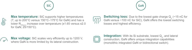
Figure 3. Key benefits of SiC and GaN semiconductors. Image used courtesy of Bodo’s Power Systems [PDF]
While both GaN and SiC offer many benefits on their own, they really shine when used together. Together, they offer a compelling blend of efficiency, compactness, and affordability in automotive power conversion systems. Designers can leverage this combination to achieve optimal power density and thermal efficiency while enabling new topologies, leading to enhanced vehicle performance and range.
Figure 4 demonstrates typical implementations of such systems.
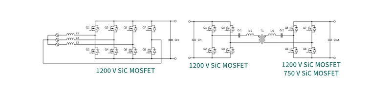
Figure 4. Schematics of 1200 V and 750 V SiC MOSFETs. Image used courtesy of Bodo’s Power Systems [PDF]
More and more tier-1 manufacturers are adopting these topologies due to their simplicity compared to the previous generations. For example, in the PFC stage of an 11 kW design, compared to 18 transistors (3x single-phase interleaved) used in Gen 1 topologies, Gen 2 topologies use only eight transistors (three-phase B6 or VSC). Just reducing the number of transistors makes the design way simpler.
EV Power System Challenges and Complexities
The new topologies use fewer gate drivers as well and enable a single microcontroller to take over the control loops of both stages of the power supply, i.e., PFC and HV-HV DC-DC. To simplify the design further, some tier-1 manufacturers have decided to eliminate discrete devices and utilize modules with three to four integrated half-bridges.
Despite considerably simplifying the design and reducing the cooling and development costs of the OBC, this approach does not optimize power density and efficiency. This is due to the huge effort required for the EMI filter design and the PFC choke, as they need to filter and switch at voltages higher than those designed for Gen 1 topologies. Certainly, at higher voltages, the switching frequencies cannot be very high (e.g., PFC 95.5 percent). Some publications have demonstrated that adding a ZVS cell to the B6/B8 topology can further increase efficiency and enable higher switching frequencies at the expense of a higher component count.
Additionally, no 900 V-1000 V aluminum capacitors are available for the output of the PFC converter. Hence, designers need to use a series-parallel arrangement of 450 V-500 V aluminum caps to achieve the capacitance necessary to store energy when the B6 topology is configured to work with single-phase grids, e.g., B8 and compensate for the 100 Hz/120 Hz ripple.
Topologies with 650 V-750 V transistors can further increase power density and efficiency at a lower system cost. Such topologies will still be compatible with three-phase grids and the 800 V battery architecture. To achieve this, multi-level converters, as shown in Figure 5, are necessary.
In Figure 5, the two topologies on the left are hard-switching PFCs, where the top image shows the flying capacitor topology and the bottom image shows an active neutral point clamp topology. The topologies on the right are resonant HV-HV DC-DC converters, where the top image shows a multilevel CLLC and the bottom image shows a multi-level DAB.
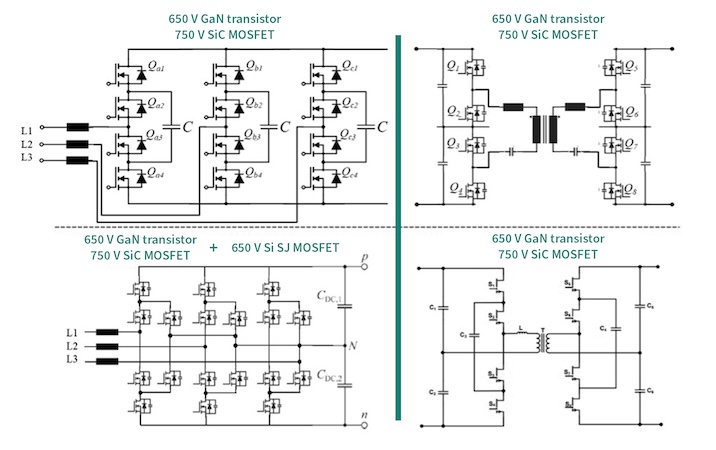
Figure 5. Multi-level converter topologies using WBG devices. Image used courtesy of Bodo’s Power Systems [PDF]
As the automotive industry continues to evolve, a sustainable design is crucial to mitigate the environmental impact of vehicles. By prioritizing eco-friendly materials, energy-efficient powertrains, and recyclable components, automotive solutions can contribute to reducing carbon emissions and conserving natural resources. In power conversion systems, this will play a crucial role in the optimization process, not only for the material selection and their recyclability but also to reduce the weight and cost of future power systems.
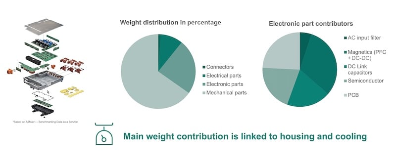
Figure 6. Weight contribution of different components in a power conversion system. Image used courtesy of Bodo’s Power Systems [PDF]
Practical GaN and SiC Implementation in Automotive Power Systems
GaN’s superior switching capabilities and high-frequency operation enable novel power electronic topologies to achieve higher efficiency and power density. GaN also reduces the overall weight of the system by reducing not only the amount of housing but also the size and number of electrotechnical components, including tons of rare materials, contributing significantly to higher sustainability.
With the introduction of the lateral structure during the manufacture of GaN power transistors, it is possible to design a bidirectional switch (BDS). Such a BDS will have bidirectional blocking voltage capability without doubling the RDS(on), enabling disruptive topologies that could bring tremendous benefits in terms of power density, reliability, cost, and external component requirements.
Figure 7 (left) shows a very modular approach that includes magnetic integration. Similar to the Gen 1 approach, each module powers each phase in the three-phase grid, enabling a 650 V device. Depending on the battery voltage, designers can select 650 V GaN or 1200 V SiC transistors.
Figure 7 (right) shows a matrix or cyclo converter – a potential candidate for innovative designs. This topology can easily be implemented with two 1200 V discrete devices connected back-to-back on the primary side and normal devices on the secondary side. The challenge here is to select low-ohmic devices to get the right total RDS(on) (the bidirectional switch has double the RDS(on) of a single device) per position, according to the proper power class and expected power dissipation.
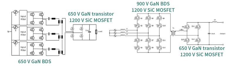
Figure 7. Modular Gen 2 approach using magnetic integration of 650 V GaN and 1200 V SiC transistors (left) and a cyclo converter. Image used courtesy of Bodo’s Power Systems [PDF]
The topology is fully resonant, and can either be an LLC or DAB, and the switching frequency range will depend on both the output load and input power-fed conditions. As this is a true three-phase topology, considering the maximum input voltage and voltage swells that may happen, the authentic bidirectional GaN switch should have a minimum breakdown voltage of 900 V. Infineon is actively working on designing an automotive BDS GaN switch such that tier-1 manufacturers are ready for mass production of these Gen 3 topologies.
Top-Side Cooling
In addition to using wide-bandgap technology to improve efficiency, device packaging and cooling become a vital part of the equation and play key roles in enabling more power-dense OBC designs. While through-hole device (THD) packages like TO-247 and TO220 are still widely used in many applications, they have the disadvantages of high manufacturing costs and of being manually inserted into the PCB before being soldered onto the underside of the board. For these reasons, THD is increasingly being replaced by surface-mount devices (SMD), the placement of which can be automated and results in higher throughput and better reliability.
SMD packages dissipate heat either by bottom-side cooling (BSC) or top-side cooling (TSC). While both BSC and TSC packages can be assembled using automated pick-and-place machinery, TSC provides several advantages over BSC packages like D2PAK and DPAK, which conduct heat generated by the die downwards towards the bottom of the board-mounted device. This direction of heat conduction is a disadvantage because PCBs are not optimized for very high heat conduction and create a substantial thermal barrier for BSC devices, requiring additional thermal vias to allow the excess heat to dissipate safely.
A negative consequence of this approach is that it makes PCB trace-routing more challenging because large areas of the board are allocated to thermal dissipation elements. An insulated metal substrate (IMS) board can improve the thermal performance of BSC devices, but these are more expensive than traditional FR4 PCBs.
The adoption of TSC technology is particularly remarkable and will shape future power-conversion system designs. In TSC devices, the heat generated by the semiconductor die is extracted from the top of the package, which has an exposed pad onto which a cold plate (heatsink) is attached, as shown in Figure 8.
This approach reduces thermal resistance by up to 35 percent and decouples the thermal pathway from the electrical connections on the PCB. This is significant as it makes PCB design simpler and more flexible, and brings the added benefits of a smaller board area, higher power density, and reduced electromagnetic interference (EMI). Furthermore, the increased thermal performance also removes the need for board stacking. So, instead of combining both FR4 and IMS boards, this design makes a single FR4 sufficient for all components and requires fewer connectors.
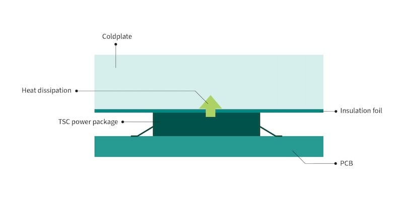
Figure 8. A semiconductor device employing top-side cooling (TSC). Image used courtesy of Bodo’s Power Systems [PDF]
These features of TSC reduce the overall bill of materials, reducing the overall system cost. TSC also helps optimize the power-loop design for increased reliability. This is made possible since the drivers can be placed very close to the power switches. The low stray inductance of the driver switch reduces the loop parasitic, leading to less ringing on the gate, higher performance, and a lower risk of failure. Furthermore, the package concept is JEDEC-compliant and free of royalties, which makes second-source manufacturing easy and available for many suppliers, while other concepts available on the market are proprietary and not easy to reproduce.
Figure 9 summarizes the key benefits of TSC technology.
Infineon has developed double (DDPAK) and quadruple (QDPAK) SMD packaging with TSC for many of its power devices, including its range of CoolSiC G6 Schottky diodes, the new SiC MOSFET family of 750 V and 1200 V devices paired with 650 V Si SJ CoolMOS, and future GaN-based CoolGaN products. Also, the low-voltage power MOSFETs are already available in TSC TOLT packages, which enables the complete system of OBC along with the DC-DC converters to be ready for TSC manufacturing. These devices offer thermal capabilities on par with THD devices and even better electrical performance.
Having a standard height of 2.3 mm for QDPAK and DDPAK SMD TSC packages, with both high- and low-voltage alternatives, helps design complete applications like OBC and DC-DC converters using components having the same height. This reduces cooling expenses compared to existing solutions based on a 3D cooling system.

Figure 9. Infineon’s top-side-cooled QDPAK platform for future power-conversion systems. Image used courtesy of Bodo’s Power Systems [PDF]
More to Explore
While SiC and GaN technologies dominate the battle to achieve greater efficiency and power density from power solutions, and they are vital to minimizing energy losses, extending driving range, and enabling faster charging of EVs, effective thermal management also plays a significant role in achieving electrical performance and reducing the size, weight, and cost of power solutions.
Innovative package designs enable top-side cooling, leading to better thermal performance than the equivalent IMS-based solution. Its simpler construction eliminates multi-board assemblies, reducing component count and cost, especially for connectors. This significantly improves performance and reduces assembly time and expenses.
There is more to explore, with several ideas for more compact, robust, and future-oriented packages in the innovation phase, with the potential to provide numerous advantages for power-conversion designers to improve power density, manufacturability, efficiency, and system cost.
Using both sides of the board significantly improves power density while reducing parasitic elements in the system. While TSC may seem ‘new,’ and in many ways it is, the USP of this solution is that it uses tried-and-tested techniques, such as gap fillers, with or without thermal interface materials, to produce an elegant and, above all, reliable solution.
This article originally appeared in Bodo’s Power Systems [PDF] magazine and is co-authored by Daniel Makus, Application and Business Development Director, and Rafael Garcia, System Architect, with Infineon.