Facebook
 Google
 GitHub
 Linkedin
Nexperia Expands Wide-Bandgap Portfolio With SiC and GaN Updates
Nexperia rolled out two wide-bandgap product updates: a top-side cooled QDPAK package for its 1200 V SiC MOSFETs, and an expanded lineup of 650 V GaN FETs in industry-standard packages.
As power converters get smaller and denser, the PCB becomes the limiting factor. Most conventional surface-mount packages depend on the board to spread heat away from the die. That means the board's thermal capacity effectively caps how much power a design can handle in a given footprint.
Nexperia’s top-side-cooled QDPAK package for its 1200 V silicon carbide (SiC) MOSFETs is aimed at high-power designs facing thermal limits. Additionally, the company has expanded its 650 V gallium nitride (GaN) FET portfolio with new RDS(on) options across industry-standard packages for industrial power conversion.

Nexperia's QDPAK package is suitable for electric vehicle charging and other high-power uses. Image used courtesy of Nexperia
The QDPAK Top-Side-Cooled Package
Nexperia’s QDPAK package has a top-side cooled, surface-mount design that creates a direct thermal path from the die to a heatsink. It separates the semiconductor's thermal management from the board's, so each can be optimized independently rather than constrained by the other.
According to Nexperia, the QDPAK’s architectural change adds meaningful headroom. Compared to conventional D2PAK-7 packaging, top-side-cooled packages can deliver up to 3 kW more output power under the same thermal constraints, while also providing around 40°C additional thermal headroom. The company also compared QDPAK to its existing X.PAK platform, stating that the new package further extends power-handling capability, enabling operation at approximately 3 kW higher power at similar operating temperatures, while providing around 23°C of additional thermal headroom at the same power level.
The QDPAK devices are available in both industrial-grade and automotive-qualified variants, with RDS(on) options spanning 17, 30, 40, 60, and 80 mΩ. The devices also carry excellent RDS(on) temperature stability along with a low-inductance package design and controlled switching behavior that support efficient operation.
An added Kelvin source pin further improves switching control and commutation speed, helping engineers manage ringing, EMI, and switching transients.
This launch is framed as a response to system-level pressure rather than a purely electrical upgrade. Target applications include EV onboard chargers, high-voltage DC-DC converters, EV charging infrastructure, photovoltaic inverters, UPS systems, motor drives, and datacenter power systems—segments where both power density and thermal margin are under constant pressure.
Expanded 650 V GaN Lineup Targets AI and Industrial Power
The GaN introduction takes a different approach. Nexperia didn't change the package architecture; it widened the RDS(on) spread inside packages the industry already uses.
The company expanded its existing 650 V industrial-grade GaN FET portfolio with RDS(on) classes—35 mΩ, 50 mΩ, and 70 mΩ—offered across TO-247-3, TO-247-4, TOLL, and TOLT packages. The 35 mΩ and 70 mΩ parts are shipping now; 50 mΩ is scheduled for Q3 2026.
That's a gap-filling move, and a useful one. Offering three resistance classes in the same standard footprints means a designer can trade efficiency (lower RDS(on)) for cost or die size (higher RDS(on)) without touching the PCB layout or redoing package qualification.

The 650 V GaN FET lineup in TOLT and TOLL packages alongside a data center. Image used courtesy of Nexperia
AI computing is driving rack power-supply requirements from sub-3 kW toward the 5-12 kW range, while renewable-energy and industrial-power systems continue to push demands for higher switching frequencies, greater efficiency, and increased power density. Nexperia positions its expanded 650 V GaN portfolio to address these trends.
To support its case, it also highlighted system-level benefits in high-power applications. In LLC converter stages used in 10-12 kW AI server power supplies, these GaN FETs can improve efficiency by approximately 0.8% to 1.2% while enabling 40% to 70% higher power density compared with silicon-based alternatives. For a typical 1 kW motor-drive system, the devices can reduce inverter power losses by around 20% to 25%, translating into an efficiency gain of roughly 1% to 1.5%.
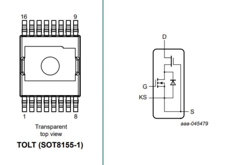
Top view of 650 V 35 mΩ GaN FET in a TOLT package with its graphic symbol. Image used courtesy of Nexperia
While the efficiency gains are notable, the power-density improvement may be the more significant advantage for many high-power applications. In AI server infrastructure, where space and power delivery are increasingly constrained, the ability to shrink magnetics and reduce overall power-supply size can be as valuable as incremental efficiency improvements.
With the expanded lineup, Nexperia aims to broaden GaN adoption across high-power applications. Target markets include data center and telecom power supplies, renewable energy systems, battery energy storage systems, and industrial drives and automation—segments that increasingly need to balance switching frequency, thermal performance, and power density simultaneously.
The Common Thread
The two launches point to a company investing in wide-bandgap power from multiple angles at once: refining the packaging around SiC die to unlock more power from existing silicon area, while broadening the format options for GaN to make it easier to drop into existing industrial designs.