Facebook
 Google
 GitHub
 Linkedin
Thermal Management for SiC Semis—Top Side Cooling as an Innovative Solution
The growing demand for powerful and compact power electronics places high demands on the thermal management of modern semiconductor technologies. Learn how SiC and GaN semiconductors in particular offer significant advantages.
This article is published by EEPower as part of an exclusive digital content partnership with Bodo’s Power Systems.
The growing demand for powerful and compact power electronics places high demands on the thermal management of modern semiconductor technologies. Silicon carbide (SiC) and gallium nitride (GaN) semiconductors in particular offer significant advantages over conventional silicon solutions, including higher voltage resistance, lower switching losses, and improved efficiency at high temperatures. However, this higher power density is accompanied by increased cooling requirements.
Traditionally, heat dissipation occurs via the underside of the semiconductor (bottom side cooling), whereby the heat loss is transferred to the housing through the substrate and the solder joint. However, multiple thermal interfaces limit the efficiency of this method. Top-side cooling is a promising alternative, in which heat is dissipated directly to a heat sink via the top of the chip. This reduces thermal resistance and improves temperature homogeneity within the semiconductor, which in turn increases the service life and efficiency of the entire system.
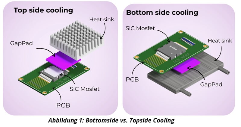
Figure 1. Bottomside vs. Topside Cooling. Image used courtesy of Bodo’s Power Systems [PDF]
A key factor for the successful implementation of top-side cooling is the selection of a suitable thermal interface material (TIM) that enables efficient heat transfer.
Challenges of Conventional TIMs for Top-Side Cooling
To optimize heat dissipation in top-side cooling, TIMs must meet several requirements: They should have high thermal conductivity, minimize thermal resistance, provide electrical insulation in most applications, and offer high mechanical stability and reliability.
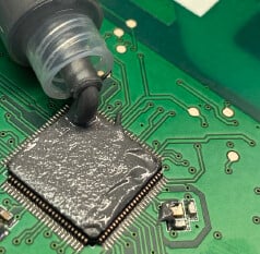
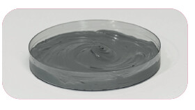
Figure 2. KERAFOL® KP 100. Image used courtesy of Bodo’s Power Systems [PDF]
Due to their low bond line thickness (BLT), thermal greases have very low thermal resistance, but they are not electrically insulating. Some of the greases available on the market also tend to exhibit the so-called “pump out effect,” especially during more intensive power cycles. The KP100 was specifically developed to significantly reduce the "pumpout effect". In general, applying paste using screen or stencil printing is very time-consuming. Pastes are also not intended for tolerance compensation; cross-linking systems such as gap filler liquids are used for this purpose.
Phase change materials (PCM) melt at higher operating temperatures, thereby reducing their contact resistance. However, they tend to be mechanically unstable over a longer period or over a higher number of cycles and can therefore lose performance. This material group is also not suitable for applications requiring electrical insulation. In addition, application of PCM requires special time-consuming assembly methods such as screen printing.
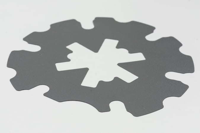
Figure 3. KERAFOL® PCM. Image used courtesy of Bodo’s Power Systems [PDF]
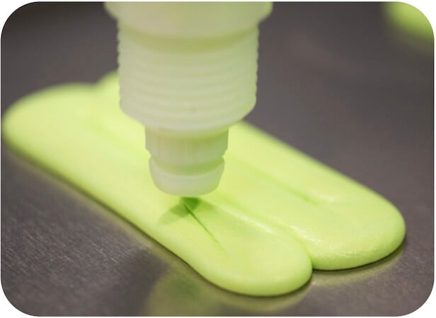
Figure 4. KERAFOL® GFL 3030. Image used courtesy of Bodo’s Power Systems [PDF]
- The use of gap filler liquids has become a popular solution, especially for l quantities. The combination of high thermal conductivity, low material costs, and easy automation using dispensing systems offers lots of advantages here. Unlike the product groups mentioned above, gap filler liquids are also electrically insulating.
The disadvantage here is the longer processing time in production due to the necessary cross-linking process of the material itself. In the case of complex geometries, the exact control of material distribution is somewhat more difficult due to the dependence on the dispensing process and component tolerances. Nevertheless, gap filler liquids are a very popular choice because they offer great advantages in tolerance compensation due to their “wet-on-wet” installation, and the mechanical pressure on the assemblies is very low. - KERAMOLD is a specially developed, thermally highly conductive, and electrically insulating granulate based on TPE, which combines the advantages of various material groups in the field of TIMs. It is applied directly to the circuit board or semiconductor chip in the overmolding process, creating a precisely fitting, thermally conductive, and electrically insulating protective layer, all without a cross-linking process.
Exkurs Hybridfolie
The trend (e.g., in the automotive industry) towards 800V architecture instead of the previous 400V poses new challenges, particularly in the area of electrical insulation strength. For safety reasons, a 2-layer TIM structure is required, for example, to ensure electrical insulation even in the event of contamination by metallic particles or air pockets. There are various possible combinations here, which are discussed in more detail in a separate application note entitled “Thermal management for SiC semiconductors in the 800V range: Top side cooling with hybrid foil.”
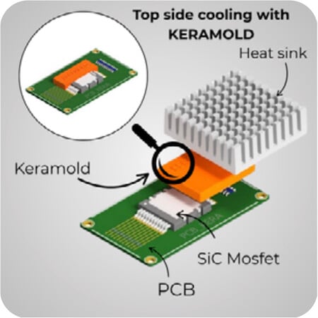
Figure 5. Topside Cooling with KERAMOLD® 15. Image used courtesy of Bodo’s Power Systems [PDF]
One option is to use a combination of thermal conductive film and gap filler liquid. Both layers are electrically insulating and thermally conductive, and the gap filler can be used to compensate for component tolerances. An alternative approach is to use a specially developed ultra-thin ceramic, which is still flexible and highly electrically insulating (approx. 5kV) with a layer thickness of only 40 μm.
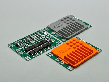
Figure 6. KERAMOLD® umspritzte Platine. Image used courtesy of Bodo’s Power Systems [PDF]
Areas of Application for Top-Side Cooling with KERAMOLD
Top side cooling in particular poses a number of mechanical, electrical, and thermal challenges. The heat dissipation of the SiC semiconductor consists of conduction and switching losses and, depending on the application, can amount to several hundred watts per module (e.g., in SiC MOSFETs for inverters in the EV industry). In addition, the requirements for insulation strength are also increasing; the electrical insulation of the TIM often has to be several kV, but this can be achieved with KERAMOLD material.
The overmolding process minimizes the contact resistance between the KERAMOLD material and the semiconductor. The high softness and elasticity of the KERAMOLD material, which, unlike conventional plastics, is in the low Shore A range, also contribute to this.
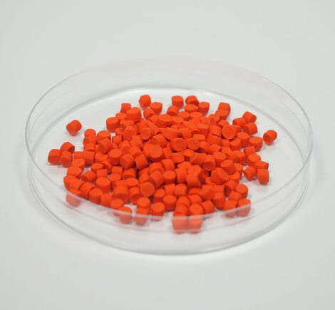
Figure 7. KERAMOLD® 15. Image used courtesy of Bodo’s Power Systems [PDF]
| ADVANTAGE | EFFECT/BENEFIT |
| HIGH THERMAL CONDUCTIVITY | Efficient heat transfer from the chip to the cooling surface |
| STANDARD FIT | 3D parts and precisely fitting encapsulation of components are possible. |
| ELECTRICAL INSULATION | High insulation resistance (protection against short circuits) |
| AUTOMATION COMPATIBLE | Reduction of process time and material usage |
High thermal conductivity: Thanks to special fillers, products in the KERAMOLD range achieve a thermal conductivity of over 2.5 W/ mK in the z-direction (through plane) and over 3.2 W/mK in the x/y direction (in plane), which is also significantly higher than conventional plastics. A material with 3.5 W/mK (KERAMOLD 35) is already in development. Improved heat dissipation and additional heat spreading allow hot spots to be cooled more effectively and, if necessary, heat sinks to be made smaller.
Precise fit: The 3D shape of the TIM not only improves heat transfer itself but also makes it easier to deal with creepage currents, as not only the contact surface of the semiconductor but also, for example, the pins are connected and encapsulated. Material utilization is also very high with this method and can be reproduced. KERAMOLD has a CTI of > 600V, which means it can be classified as insulation class I and can help to keep component spacing small.
Excellent mechanical strength: Overmolding with soft and elastic TPE provides additional protection for the semiconductor chip against mechanical stresses such as vibrations or CTE mismatch, moisture, and environmental influences, which extends the service life of the electronic components.
All-in-one solution: Thanks to the complete encapsulation of the circuit board and the SiC semiconductors, other materials and process steps such as potting or conformal coating are no longer necessary, as the KERAMOLD material was developed not only for heat transfer but also for protection of the electronic assembly.
Figure 8. KERAMOLD® 25. Image used courtesy of Bodo’s Power Systems [PDF]
Conclusion
KERAMOLD is a key technology for efficient top-side cooling. The requirements in the field of power electronics are very complex and individual. Therefore, it is not possible to say in general terms which TIM group should be used, as this depends on many factors.
Nevertheless, KERAMOLD definitely represents a new approach here and gives developers new degrees of freedom.
By directly overmolding the semiconductor with a thermally conductive protective layer, considering a reduced process time in the manufacturing, heat dissipation, electrical insulation, and mechanical stability are all optimized. The KERAMOLD product range shows its greatest advantage when, in addition to protecting the electronics, an improvement in thermal performance is also required. The performance of KERAMOLD can and will be further improved, which is still necessary for some applications.
This article originally appeared in Bodo’s Power Systems [PDF] magazine.