Facebook
 Google
 GitHub
 Linkedin
Powering the SiC Revolution with Vertical Integration
Silicon Carbide (SiC) has a 3x bandgap compared to silicon. Learn how unipolar devices like MOSETs in the several kV range are possible with SiC.
This article is published by EEPower as part of an exclusive digital content partnership with Bodo’s Power Systems.
SiC is Revolutionizing the Power Semiconductor Market
Unipolar devices such as MOSFETs usually offer lower conduction (under partial load conditions) and switching losses making them attractive for many applications such as Photovoltaics (PV) and Automotive Traction Inverters. As a result, SiC based devices have already penetrated the market, with a market share that is expected to reach close to 10B$ at the end of the decade with a CAGR of over 30%, thereby revolutionizing the power semiconductor market.
Silicon Carbide is not Silicon!
However, the manufacturing of SiC is significantly different from Silicon. E.g., SiC monocrystal is usually grown by sublimation unlike Si which is usually grown from a melt. Furthermore, the processing of SiC wafers is more challenging owing to its higher hardness and brittle nature, compared to Si. Also, SiC usually involves higher processing temperatures. All these factors not only make the entire process significantly more expensive compared to Si, but also result in a higher defect density compared to Si. This is why a strong understanding of the complete process all the way from crystal growth to device fabrication and packaging is crucial for success in SiC.
Sanan Benefits from 20+ Years of Compound Semiconductor Expertise
Sanan Semiconductor benefits from a strong knowhow of compound semiconductors, stemming from its 20+ years of expertise in semiconductors such as GaAs, GaN, InP, LN, LT etc., catering to markets such as optoelectronics, RF, optical devices and Power semiconductors, each of the semiconductors for which Sanan is today vertically integrated.

Figure 1. Sanan’s Vertically Integrated State-of-the-art 150 and 200 mm SiC Mega Factory. Image used courtesy of Bodo’s Power Systems [PDF]
Vertically Integrated State-of-the-Art 150 and 200 mm SiC Mega Factory
In 2020, Sanan established a state-of-the-art vertically integrated SiC mega factory (Figure 1) with a planned capacity of around halfa-million wafers annually. Built with an investment of over $2B, this fab caters to producing SiC, all the way from substrates to packaged products, in both 150 mm and 200 mm. This makes it possible to cater to a wide base of customers, at different stages in the value chain. As a result of vertical integration, Sanan maintains the complete supply chain thereby leveraging its capacity, cost and quality advantages.
200 mm Substrates and Epi-Wafers Released for Mass Production
Sanan has developed the processes in-house to mass produce SiC powder, which is the raw material for substrate production, with a purity of 6N grade (99.9999%). This is crucial to producing SiC substrates with low defect densities, which is necessary to reach high levels of yield in device fabrication. 150 mm substrates have been in mass production since 2021, and Sanan leveraged this experience also to 200mm (see Figure 2), which have been released for mass production this year.
SiC devices are usually fabricated on an epitaxial layer, which serves as the drift region, grown on the substrate. A good epitaxial process not only prevents new defects forming in the drift layer, but also stops any remaining killer defects present on the substrate from expanding into the drift region. Therefore, high quality epitaxy is crucial to fabricating devices in high volume at high quality. Epi-wafers have been released for mass production, in 150 mm as well as 200 mm.
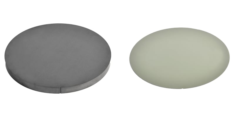
Figure 2. 200mm SiC Boule (left) and Substrate (right) released for mass production. Image used courtesy of Bodo’s Power Systems [PDF]
Over 200 Million SiC Devices Shipped for Various Applications
Three generations (G1, G2 and G3) of SiC schottky diodes have already been released to the market, in a wide portfolio ranging from 2-60A, in voltage classes from 650V-2kV in various standard packages, for industrial as well as for automotive markets. Different applications usually have different trade-offs. For example, outdoor applications such as solar usually need higher surge current capability.
On the other hand, power supply applications need the lowest forward voltage. Keeping this in mind, two flavours of the G3 diode have been tailor-made to meet the above applications, namely the “higher-surge” version and the “Low Vf” version, in addition to the “General Purpose” version. A popular application example for SiC Schottky diodes is a classical boost Power Factor Correction (PFC) converter, where replacing the Si diode with a SiC schottky diode helps to cut down the reverse recovery losses in the diode and the turn-on losses in the active switch, thereby enhancing the system efficiency by 0.5 p.p (Figure 3). Moreover, both the diode and active switch operate at a significantly lower temperature [1].
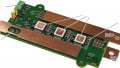
Sanan has already released the Gen-1 SiC MOSFETs based on the planar structure (Figure 4) targeting industrial and automotive applications. Subsequently, cell engineering of the above planar structure has lead to significant improvements in the RDS*A Figure-of-Merit (FOM) which is available as Gen-2 (released) and Gen-3 (to be released later in 2025).
Current portfolio extends from RDS(on) classes of 10 mΩ - 1000 mΩ, in voltage classes 650 V, 750 V, 1200 V, 1700 V and 2000 V, industrial and automotive qualified devices, available as bare dies, standard discrete packages such as TO-247, D2PAK, top-side cooled, and customer specific modules [2]. Furthermore, a trench structure (in early development), and a super-junction MOSFET (in early concept development) are expected to significantly enhance the FOM of the SiC mosfets, bringing them closer to Si devices in terms of cost-performance.
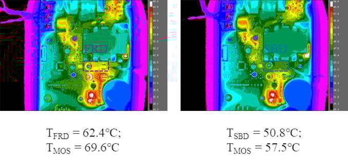
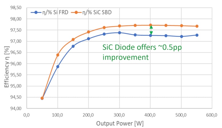
Figure 3. Replacing the Si diode in a Boost-PFC Converter with a SiC Schottky diode helps enhance system efficiency by 0.5 p.p (bottom) and the diode and active switch operate cooler (top: left Si, right SiC). Image used courtesy of Bodo’s Power Systems [PDF]
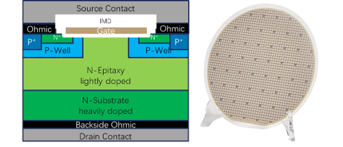
Figure 4. Automotive Qualified SiC Planar MOSFETs Technology currently in Mass Production. Unit cell (left) and bare-die wafer (right). Image used courtesy of Bodo’s Power Systems [PDF]
Chip Capabilities Complemented by Packaging Capabilities
To reap the superior performance of SiC devices, it is imperative to have enabling packaging technologies which allow, e.g., lower parasitic inductances, better cooling, better layout for good current sharing. Being a vertically integrated supplier, Sanan has in-house capabilities not only for many state-of-the art-packages, but also for customer-specific packages. This can enable customers to reach their required levels of performance at desired costs, thus bringing the benefits of vertical integration to help power the SiC revolution.
Sanan SiC Mosfets Demonstrate 99.6% Efficiency in a Softswitching Inverter Topology
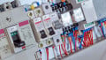
To demonstrate their performance in an application, Sanan SiC Mosfets were tested in an inverter application (Figure 5). The topology used in this case is the Single Shared Inductor Auxiliary Resonant Commutated Pole (S²I-ARCP) [3], which is a soft-switching topology. The main branch, which carries the load current, was populated with 1200V 16 mΩ SiC MOSFETs in TO-247 package (SMS1200016M2) [4]. The auxiliary branch, which is responsible for the soft switching and which carries only a small fraction of the load current was populated with 1200V 20 mΩ SiC MOSFETs (SMS1200020M2) [5] though even higher-RDS(on) devices would have sufficed. These devices have been optimized for soft switching, by enabling a higher switching speed.
Figure 6 shows the measured efficiency at dc link voltage Vdc= 800 V, output voltage V0,rms= 230 V, output frequency fel = 50 Hz and switching frequency fsw = 30 kHz, and it can be seen that the peak efficiency exceeds 99.6%, demonstrating the performance of the SiC MOSFETs. Figure 7 compares the measured temperature in the case of hard switching and soft switching. It can be seen that the main switches (Pu1) operate significantly cooler in the case of soft switching. Of course, some of the losses are moved to the auxiliary switches (Pu2 and Pu3), but they are insignificant compared to the savings in the main switches.
NOTE: Further details on this topology and measurements will be presented in more details in a future article.
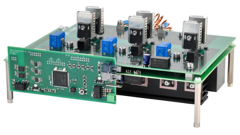
Figure 5. S²I-ARCP Soft-switching Inverter populated with SiC MOSFETs from Sanan Semiconductor. Image used courtesy of Bodo’s Power Systems [PDF]
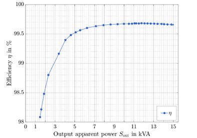
Figure 6. Measured Efficiency in the S²I-ARCP Softswitching Inverter populated with SiC MOSFETs from Sanan Semiconductor. Vdc= 800 V, V0,rms= 230 V, fel = 50 Hz, fsw = 30 kHz. Image used courtesy of Bodo’s Power Systems [PDF]
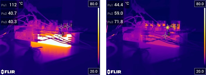
Figure 7. Measured Temperatures in the S²I-ARCP Soft-switching Inverter populated with SiC MOSFETs from Sanan Semiconductor. Vdc= 800 V, V0,rms= 230 V, fel = 50 Hz, fsw = 30 kHz. (Left: without soft-switching, right-with soft-switching). Image used courtesy of Bodo’s Power Systems [PDF]
References
[1] “Silicon Carbide Schottky Barrier Diodes”, Application Note, Sanan Semiconductors
[2] “Silicon Carbide Power Products”, Product Brief, Sanan Semiconductors
[3] T. Lehmeier, A. Amler, Y. Zhou, and M. März, “Three-Phase ARCP Inverter Using Soft-Switching With a Single Shared Inductor,” IEEE Trans. Power Electron., vol. 39, no. 2, pp. 2505–2521, 2024.
[4] Datasheet, SMS1200016M2 1200V 16mΩ Silicon Carbide Power MOSFET, Sanan Semiconductor
[5] Datasheet, SMS1200020M2 1200V 20mΩ Silicon Carbide Power MOSFET, Sanan Semiconductor
This article originally appeared in Bodo’s Power Systems [PDF] magazine and is co-authored by Ajay Poonjal Pai, Head of Innovation, Sanan Europe, and Thomas Lehmeier, Yan Zhou, Institute of Power Electronics, Friedrich-Alexander University of Erlangen-Nuremberg.