Facebook
 Google
 GitHub
 Linkedin
Revolutionizing Circuit Protection With SiC JFETs
Traditional circuit breakers have limitations, but advances have led to significant improvements.
This article is published by EEPower as part of an exclusive digital content partnership with Bodo’s Power Systems.
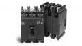
The mid-20th century saw significant innovation in residential and industrial electrical systems. One of the most impactful advancements was the transition from traditional replaceable fuses to miniature circuit breakers (MCB). While fuses provided basic protection, they had to be replaced after they blew. Circuit breakers, on the other hand, could be easily reset after tripping. This convenience led to building codes and electrical standards favoring circuit breakers over fuses in new construction.
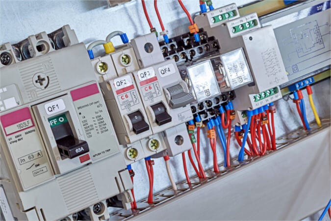
Image used courtesy of Adobe Stock
Trends in Circuit Breakers
Innovations such as ground fault circuit interrupters (GFCI) and arc fault circuit interrupters (AFCI) have further enhanced circuit breakers over the years. Despite these improvements, traditional circuit breakers still have limitations because of their mechanical relays. These limitations include:
- Arcing: When relay contacts open or close, arcing can occur, which is especially problematic during circuit faults with high currents.
- Disconnect speed: The speed at which an electromechanical circuit breaker disconnects is limited by the physics of its coil and the relay’s inertial mass.
- Wear and tear: Over time, the contacts in a mechanical relay wear out, limiting the number of interruption cycles.
The current trend is a new type of circuit breaker that replaces the electromechanical relay with semiconductor power devices, known as solid-state circuit breakers (SSCB) or semiconductor circuit breakers (SCB). These SSCBs offer several advantages:
- Arcing: Semiconductor switches connect and disconnect without producing arcs, eliminating the need for special arc-suppression features.
- Disconnect speed: Free from the constraints of a magnetic coil, semiconductor switches can operate hundreds of times faster than electromechanical relays. This rapid response allows current to be interrupted before it becomes hazardous, which is crucial for effective circuit protection.
- Wear and tear: Because they do not have mechanical components, semiconductor switches can perform unlimited connect/disconnect cycles without degradation.
The transition from incandescent to LED lighting offers a useful analogy for the transition from electro-mechanical to semiconductor circuit breakers. The widespread adoption of LED bulbs that could be installed into existing sockets designed for incandescent bulbs allowed customers to gradually make the transition. In the early years, when LED lighting had a high price premium, users could install LED bulbs only in high-use sockets where the efficiency gains justified the additional cost.
Semiconductor Circuit Breaker Challenges
Similarly, the development of SCBs installed directly into electrical panels originally designed for electro-mechanical circuit breakers will allow a gradual methodical transition. However, this introduces significant challenges, the first of these being thermal management. Traditional circuit breakers based on mechanical relays have extremely low contact resistance, producing little heat during normal operation. Consequently, circuit breaker panels have minimal accommodations for the removal of heat, with limited airflow and no heat sinks. Given these constraints, SCBs designed for existing panels must generate minimal heat, necessitating a low effective on-resistance of the semiconductor switch.
The second challenge for SCBs is size. To be compatible with existing panels, SCBs must conform to the form factor of existing electro-mechanical circuit breakers, limiting the number of devices that can be installed in parallel to achieve the target resistance defined by the thermal constraints of the circuit breaker panel. These constraints drive the need for ultra-low RDS(on) devices in compact packages.
Qorvo’s SiC JFET meets these stringent requirements with the lowest on-resistance by area (RDS·A) figure of merit of any device type in its voltage range, thanks to its simple structure.
Figure 1(a) shows a simplified cross-section of a Qorvo SiC JFET with gate-source voltage VGS = 0 and drain-source voltage VDS nearly zero. This represents one of the thousands of parallel cells in a JFET chip with terminals labeled Source, Gate, and Drain. The Qorvo SiC JFET has two PN junctions, thus two diodes: drain-to-gate and gate-to-source, shown in the figure superimposed across the corresponding PN junctions. In this unbiased state, a highly conductive channel exists between the Drain and Source, allowing electrons to freely flow in either direction, yielding the distinctive low on-resistance of the Qorvo SiC JFET.

(a)

(b)
Figure 1. Vertical JFET cross section (a) without bias voltages, and (b) biases for VG(th) characterization. Image used courtesy of Bodo’s Power Systems [PDF]
Around each PN junction is a highly resistive depletion region, as mobile carriers have been repelled from the PN junction. The drain-gate depletion regions are indicated as gray areas in Figure 1. In (b), applying enough drain-source voltage motivates current to flow. However, the current is almost zero, blocked by the expansion of the depletion regions due to the application of a negative gate-source voltage. When these depletion regions meet, the channel is pinched off.
The Qorvo SiC JFET is normally on (fully conductive) with no gate-source voltage applied and requires a negative VGS to switch and remain off. While some semiconductor-relay applications benefit from this normally-on state, most require a default normally-off state. The normally-on Qorvo SiC JFET works well for both types, as the addition of a few simple components can keep it in a normally-off state, even without control power. But first, a couple of graphs can help understand the construction of the Qorvo SiC JFET.
Shown in Figure 2(a) are output characteristics with various gate-source voltages at room temperature of a 750 V, 4.3 mΩ SiC JFET in a TOLL (MO-229) package, part number UJ4N075004L8S. The typical part has a gate threshold voltage VG(th) = -6V.
With VGS = -5V, the channel width is highly constricted by the depletion regions, so current flow is limited. Current increases slightly with VDS, and the JFET is in “saturation.” At VGS = -4V, the depletion regions are narrower, making the channel wider and thus increasing conductivity (reducing the on-resistance). This curve shows the effect of increasing VDS and widening the depletion regions, bending the output characteristic curve until there is little increase in current versus VDS. On the other hand, increasing VGS decreases the width of the depletion regions, which widens the channel and increases conductivity. The figure shows curves corresponding to certain VGS values all the way to +2V, which is the last VGS test voltage.

Figure 2. UJ4N075004L8S (a) output characteristics at 25°C, and (b) gate current versus VGS. Image used courtesy of Bodo’s Power Systems [PDF]
Note that in these figures, RDS(on) is on-resistance characterized at either VGS = 0V or VGS = +2V. A slightly positive VGS, such as 2 to 2.5 V, further shrinks the drain-gate depletion regions and reduces RDS(on) by 15%, depending on operating conditions. Commonly called overdriving, it’s an easy way to minimize JFET RDS(on) without risk of damage or parameter drift — yet another advantage of the Qorvo SiC JFET in applications that require cool operation and a long service life.
The on-resistance temperature coefficient (TC) is positive, which, combined with controllable switching speed via the gate drive, makes paralleling easy. However, the strong TC must be considered when selecting parts and deciding how many to parallel. Even at high operating temperatures, Qorvo’s SiC JFET has substantially lower conduction loss per package size compared to competing device technologies.
Figure 2(b) shows the gate current versus VGS for Qorvo’s UJ4N075004L8S, where the SiC JFET gate-source diode is forward-biased. The temperature-dependent diode “knee voltage” is clearly visible, and the slope corresponds to the JFET gate resistance, which is 0.4 Ω. VGS is in a range of 2 to 2.6 V with IG in the milliamps range and temperature spanning from -55 to 175°C. This graph also shows the JFET’s gate-source diode forward voltage temperature coefficient of -3.2 mV/°C, which can be used to sense the JFET chip temperature with a simple differential amplifier circuit.
The simple structure of the Qorvo SiC JFET yields unrivaled conductivity, but this simplicity also delivers unmatched reliability and durability. Current flows directly through SiC material that is doped with highly mobile electrons. There is no PN junction in the current path, nor is there surface current. This design ensures no degradation mechanism, hysteresis, or unusual dynamic effects. Additionally, a burn-in is not needed. As long as safe operating conditions are not grossly exceeded, the Qorvo SiC JFET’s operation remains consistent even after many years.
One final trait results from the simplicity of the Qorvo SiC JFET structure—robustness. The SiC material can withstand high internal temperatures, hundreds of degrees Celsius, without parameter shift, provided the energy remains within safe limits. This enables the Qorvo SiC JFET to switch off very high currents, including short circuits, for any number of cycles. Electromechanical circuit breakers and relays endure a limited number of emergency-switching cycles, sometimes only one.
Figure 3 shows a bidirectional blocking configuration with a simple overdrive of the JFETs. This circuit is normally on, meaning that the JFETs are on when there is no gate drive power. An off-the-shelf gate driver directly drives each JFET gate with no need for voltage regulation. The value of the on-state resistor depends on the desired JFET gate current; at least 1 mA is enough to overdrive the JFET gate, while 5 mA or more is recommended for easy on-chip temperature sensing. Note that the switch-on speed is relatively slow with the large on-state gate resistance, but this is desirable for many SCB and relay applications.

Figure 3. Direct drive circuit with bidirectional blocking and normally on state. Image used courtesy of Bodo’s Power Systems [PDF]
The JFET gate driver’s negative supply voltage can range from a minimum -30 V to a recommended maximum of -12 V for VSS or an absolute maximum of 2 V below the SiC JFET’s minimum threshold voltage value specified in the datasheet. The positive supply voltage depends on the selected gate driver’s undervoltage lockout (UVLO) rating. For example, a gate driver such as UCC5304 can have as little as 6 V for VDD, allowing for adjustment of the on-state gate resistance accordingly.
Figure 4 shows a bidirectional blocking configuration, again with a simple overdrive of the JFETs. A normally-off state is achieved by connecting a low-voltage silicon MOSFET in series with each JFET in a quasi-cascode configuration. An off-the-shelf gate driver directly drives each JFET’s gate, while a voltage supervisor controls each MOSFET, ensuring they remain on when the gate drive supply voltage is within operating range. The voltage supervisor in the block diagram monitors the negative gate drive voltage, so the MOSFET remains off until the JFET can be reliably switched off by the JFET gate driver. Alternatively, the voltage supervisor could be substituted by a gate driver.
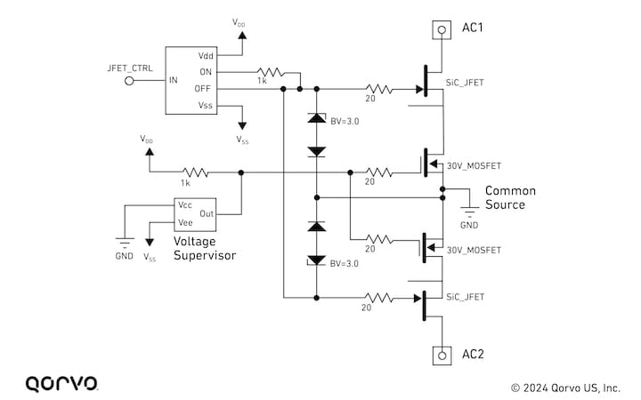
Figure 4. Direct drive circuit with bidirectional blocking and normally off state. Image used courtesy of Bodo’s Power Systems [PDF]
Similar to the circuit in Figure 3, the JFET’s switch-on is through a large value gate resistor. The JFET gate-source diodes have a temperature-dependent forward voltage of 2 V to 2.5 V. Thus, the Zener diodes, with a breakdown voltage (BV) of 3V, will not activate, allowing 6 mA to flow into each JFET.
The diodes in anti-series with the Zener diodes allow the gate driver to pull the JFET gates negatively. During normal operation, it is as if these diodes and the Zener diodes are effectively bypassed. Their main purpose is to switch off the JFETs in the absence of gate drive power, such as during startup. In this circumstance, as the voltage rises across the AC power terminals, the voltage rises across the normally-off MOSFETs. When the voltage exceeds the Zener BV plus the magnitude of the JFET threshold voltage, the JFETs are off, so no current flows, even if the voltage across the AC terminals reaches several hundred volts.
The JFET drive examples here are just a few of the many possible implementations. Key points are:
- Simple gate drive for both normally-on and -off configurations
- Design flexibility
- Use of readily available gate drivers and circuit components
A bonus feature of directly driving the JFET gate is on-chip temperature sensing using the JFET’s gate-source diode. This TJ sense method uses the JFET chip itself, eliminating the need for a sense diode or other device either inside or outside the JFET package. This means that the temperature sensing is both highly accurate and responds quickly.
Figure 5 shows a differential amplifier that measures the JFET gate-source voltage VGS. It includes a part of the gate drive circuitry from Figure 4, though some optional components are omitted for clarity, such as input-filtering capacitors and voltage clamp diodes. The amplifier in Figure 5 has unity gain because VGS varies within the range of many analog-to-digital converters (ADC) built into microcontrollers. To mitigate high-frequency noise, a resistor-capacitor filter is used to smooth the amplifier output before transmitting the T_SENSE signal to an ADC input. The RC filter capacitor must be as close to the ADC input as possible.
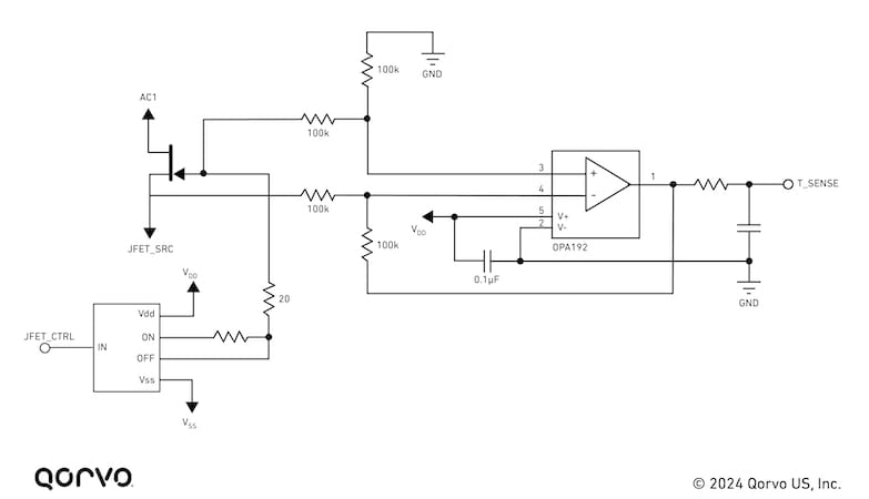
Figure 5. Temperature-sensing amplifier. Image used courtesy of Bodo’s Power Systems [PDF]
This circuit can only sense the JFET chip temperature while the JFET is on and being overdriven. Note that regulating the current into the JFET gate, or the gate supply voltage, is unnecessary. For example, suppose the output of the gate driver is 15 V, and the on-state gate resistance is set so that 6 mA flows into the JFET gate. At that gate current, Qorvo’s UJ4N075004L8S JFET has a VGS temperature coefficient of -3.2 mV/°C. The JFET VGS self-regulates based on chip temperature with a maximum range of 0.736 V for a temperature span of 230°C (-55 to 175°C). A usual temperature span would be about 100°C, corresponding to a range for VGS of about 0.32 V, which is very small compared to the +15 V drive voltage. Therefore, the current into the JFET gate can be considered constant with little error in the temperature measurement. This is a very simple, low-cost circuit that, along with overdriving, takes full advantage of the Qorvo’s SiC JFET features.
The Future of Circuit Protection
Imagine today that there are no existing circuit protection products, and they must be developed from scratch. In this race to market, electromechanical breakers are in one lane, and semiconductor circuit breakers are in the other. Which one wins? Your answer to that question could shape the future of circuit protection.
This article originally appeared in Bodo’s Power Systems [PDF] magazine and is co-authored by Jonathan Dodge, P.E., Principal Applications Engineer, and Andy Wilson, Senior Business Development, Qorvo.