Facebook
 Google
 GitHub
 Linkedin
A Three-Phase 3-level Flying Capacitor DC-AC Converter Based on GaN FETs
This article examines the deployment of gallium nitride (GaN) field-effect transistors (FETs) featuring integrated gate drivers in a three-phase three-level DC-AC converter.
This article is published by EEPower as part of an exclusive digital content partnership with Bodo’s Power Systems.
Power-conversion systems in renewable energy face increasing demands for both high efficiency and compact design. This requirement has established FETs based on GaN technology as a preferable solution for single-phase applications operating at 400 VDC link voltages [1], [2]. GaN devices offer advantages over traditional silicon semiconductors because their faster switching speeds reduce switching losses.
The challenge emerges when transitioning to 800V systems. As system voltages increase, this voltage stress becomes a critical constraint that makes it hard to adopt GaN technology in higher-voltage applications, despite its superior switching characteristics. Multilevel converter topologies provide a solution by distributing voltage stress across multiple switching devices through the strategic addition of active and passive components [3].
Among the multilevel topologies documented in literature, the flying capacitor configuration emerges as the most cost-effective solution [3]. This topology achieves an optimal balance between FET voltage stress reduction and implementation complexity, making it particularly suitable for applications requiring both performance and economic viability. Furthermore, the flying capacitor topology’s results are agnostic to the power factor, thus making it suitable for all inverter or power factor correction (PFC) applications.
In this paper, I will experimentally assess the performance of the three-level flying capacitor topology with a specific focus on implementation using Texas Instruments (TI) GaN FETs that have an integrated gate driver in the slim transistor-outline leadless top-side (STOLT) package.
Topology Consideration
Figure 1 is a schematic representation of a three-phase three-level flying capacitor converter. From left to right, the system comprises a DC current source, three flying capacitor switching cells, switching inductors, an electromagnetic interference filter, and a connection to the three-phase grid by means of a point of common coupling. The AC phases are labeled L1, L2 and L3, with positive currents exiting the converter. The DC side features positive and negative rails for a current generator operating as a source or a load.
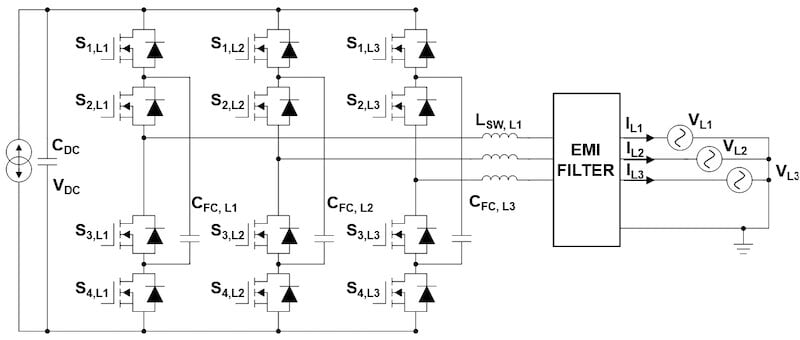
Figure 1. A schematic representation of a three-phase DC/AC converter based on three-level flying capacitor switching cells. Image used courtesy of Bodo’s Power Systems [PDF]
The single switching cell comprises:
- Four power FETs rated for half the DC link voltage (S1, S2, S3, and S4).
- The flying capacitor (CFC). This capacitor is rated for half the DC link voltage, and its value is inversely proportional to the switching frequency [4].
- The DC link capacitor is responsible for filtering out the ripple current (CDC).
- A switch-node inductor with one-fourth the required inductance of two-level applications [4].
This DC/AC converter requires compliance with the following condition (Equation 1):
\[V_{DC}>\sqrt{2V_{AC}}\,\,\,\,\,(1)\]
where VAC represents the root-mean-square (RMS) line-to-line voltage.
Operating Principles of a Flying Capacitor Switching Cell
In the flying capacitor topology, a microcontroller (MCU) needs to control the flying capacitor voltage at a value half the DC link voltage. This specification avoids any possible overvoltage across the FETs. The MCU imposes the duty cycle and dead time so that the FETs switch at a nominal switching frequency (fSW).
Switch pairs S1 and S4 and S2 and S3 are switching complementary to each other. Two pairs of dead times are required per switching cell. If these switch pairs are not complementary to each other, CDC may short.
Switch pairs S1 and S4 and S2 and S3 are 180 degrees phase-shifted to each other. The phase shift doubles fSW on the switching node.
Switch pairs at first approximation have the same duty cycle, expressed by Equation 2:
\[D=\frac{V_{SW}}{V_{DC}}\,\,\,\,\,(2)\]
where VSW is the voltage with negative DC rails as a ground reference.
Figure 2 shows the pulse-width modulation (PWM) signals and switch-node voltage when 920V on the switch node is present with 1,000VDC. In this condition, the duty cycles are 92% (S1 and S2). The switch-node voltage is switching within two levels – 500V and 1,000V – because the duty cycles are >50%.
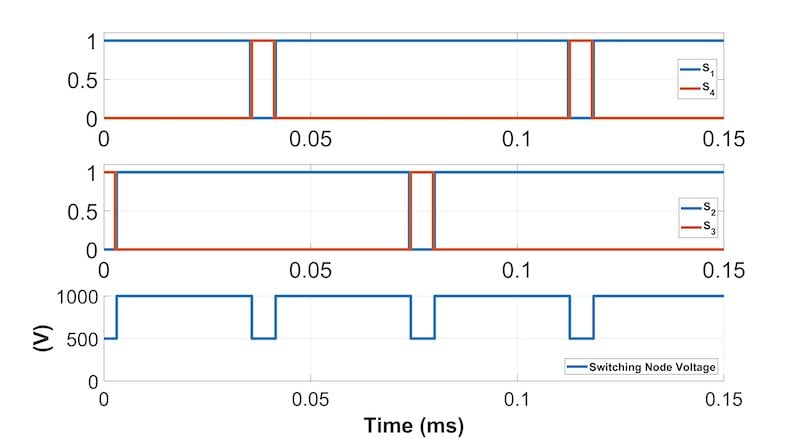
Figure 2. Simulation results – MCU PWM signals and switch-node voltage at 1,000VDC, 920V and a 92% duty cycle. Image used courtesy of Bodo’s Power Systems [PDF]
Flying Capacitor Layout Considerations
Maximizing fSW is crucial for reducing flying capacitor capacitance [4]. Power devices such as GaN FETs enable both high fSW and high efficiency, but there are design challenges. Higher switching frequencies inherently result in an elevated current slew rate, which, when combined with parasitic loop inductance, creates substantial device overvoltage that can lead to catastrophic device failure. In multilevel converters, the spatial separation between control circuits and switching devices compounds the problem by increasing the parasitic loop inductance and compromising FET gate control.
Figure 3 is a schematic representation of parasitic loop inductances within a three-level flying capacitor switching leg. The switching cell features two distinct commutation loops that significantly impact overall performance.
The inner commutation loop, indicated by blue arrows, encompasses the parasitic inductances of switches S2 and S3 and the inner capacitor (CINNER). This loop offers substantial optimization potential through strategic component placement, where positioning elements in proximity effectively minimizes the parasitic inductance.
In contrast, the outer commutation loop depicted by the red circle comprises switches S1 and S4, the outer capacitor (COUTER), and CINNER, forming the external switching path. Since the inner loop has already been optimized for minimum inductance, achieving simultaneous optimization of the outer loop presents considerable design challenges. Strategically positioning an additional capacitor (CADD) in electrical parallel with switches S2 and S3 reduces the overall parasitic effects to their minimum achievable values [5].
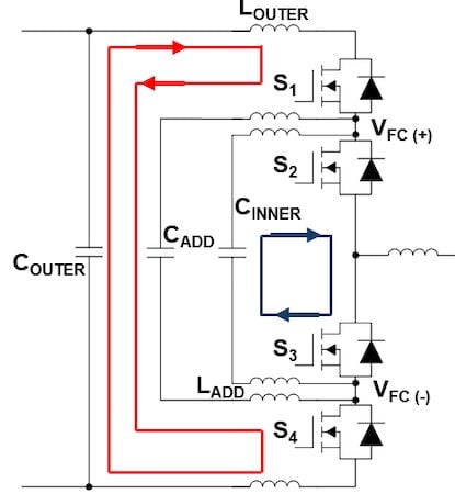
Figure 3. Commutation loops of a three-level flying capacitor switching cell. Image used courtesy of Bodo’s Power Systems [PDF]
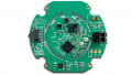
Figure 4 demonstrates a practical implementation of this optimization strategy using GaN devices in the STOLT package. Figure 4a reveals the presence of three ceramic capacitors. The addition of CADD results in significant improvement of the switching loop performance characteristics. However, as evident from Figure 4b, incorporating additional components increases overall board dimensions and introduces complexities in gate-driver signal management.
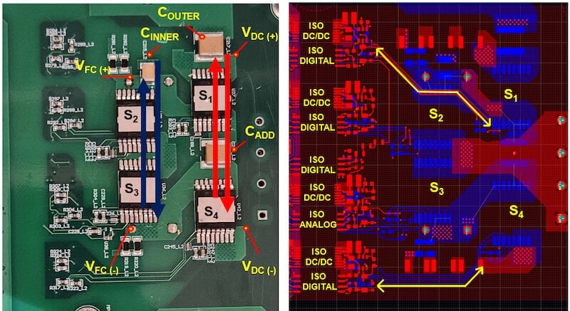
Figure 4. Bottom view of a flying capacitor switching leg plus printed circuit board layout view (top and bottom layers). Image used courtesy of Bodo’s Power Systems [PDF]
While this signal management complexity frequently necessitates derating the switching speed – resulting in increased total losses that offset the advantages gained from higher fSW – it is possible to mitigate losses by implementing transistors with integrated gate drivers, such as the TI LMG3670R010. This gate driver’s integrated architecture enables GaN transistor switching performance by leveraging an internally optimized gate-driver design, eliminating many of the layout-dependent parasitic effects that compromise discrete implementations.
While integrated gate drivers address switching-related parasitics, auxiliary components can become performance bottlenecks. Components such as isolated DC/DC converters for gate-driver power supplies, voltage sensors for flying capacitor voltage sensing, and digital isolators for control signals must feature superior common-mode transient immunity to maintain signal integrity. Components such as TI’s UCC35131, AMC0311D and ISO7721 exemplify the specifications required to preserve the high-frequency switching advantages of integrated GaN solutions.
Experimental Results
The TI 15kW to 30kW Bidirectional, Three-Phase Plus Neutral Flying Capacitor Based on GaN Reference Design (https://www.ti.com/tool/ TIDA-010957) can evaluate the performance of a three-phase flying capacitor DC/AC converter [6]. This design is capable of delivering 30kW using GaN devices in the STOLT package with an on-resistance value of 10mΩ. The converter is operating at 65kHz by having a controlled switching speed of 70V/ns.
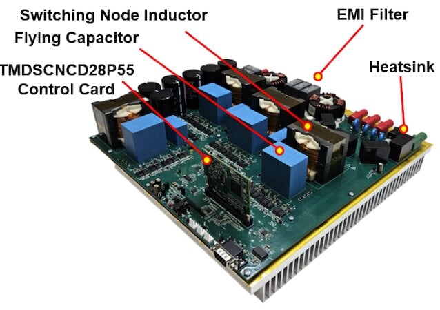
Figure 5. Lateral view of the hardware prototype board of the 15kW-to-30kW bidirectional reference design, where LMG3670R010 connects directly to the heat sink. Image used courtesy of Bodo’s Power Systems [PDF]
Power vs. Efficiency Measurements
This experiment kept the DC bus voltage constant and controlled at 800VDC. AC connected first at 480VRMS and later at a 400VRMS power grid.
Figure 6 shows the current and voltages of one phase of the DC/AC converter operating at full power. The converter is operating as a PFC. The switch-node voltage shows three distinctive levels when considering the electrical frequency grid period. This is because half of the period requires a duty cycle 50%. Having three voltage levels plus doubling the equivalent fSW enables the grid current to have low ripple current.
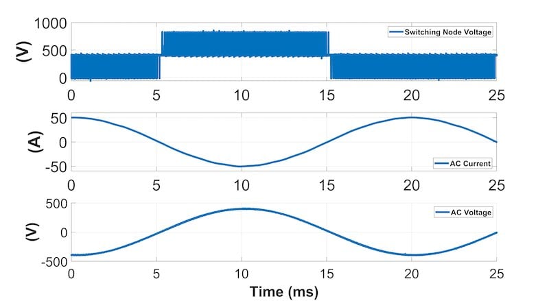
Figure 6. Experimental waveforms of the reference design operating at 30kW with a grid connection at 480VRMS. Image used courtesy of Bodo’s Power Systems [PDF]
Additional tests at different power factors but the same apparent power value indicated no significant worsening in ripple current or total losses.
Subsequently, varying the DC/AC converter power from 2.5kW to 30kW enabled measurement of the corresponding efficiencies at each operating point. Figure 7 depicts efficiency vs. power curves for two different grid voltage levels. At first observation, it is evident that both efficiency and power performance at 480VRMS are superior compared to 400VRMS operation.
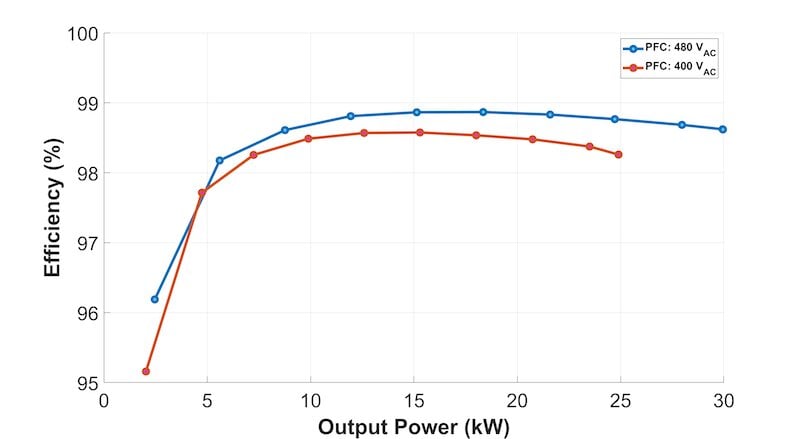
Figure 7. Efficiency vs. power at 800VDC and two different line-to-line grid voltages. Image used courtesy of Bodo’s Power Systems [PDF]
Operating at 480VRMS at the maximum power output of 30kW resulted in a peak efficiency measurement of 98.7%. While there were lower efficiencies during 400VRMS operation, these results remain impressive. The performance difference occurs because, for equivalent RMS current levels, the losses remain similar while the power-transfer capability is higher at the elevated voltage, resulting in improved overall efficiency at 480VRMS operation.
Conclusion
Flying capacitor topologies are preferable when trying to decrease converter size and increase efficiency. Adopting GaN transistors can significantly increase fSW, making this topology even more appealing. Using TI GaN FETs with integrated gate drivers optimizes power layout, achieving a switching speed of 70V/ns with no significant voltage overshoot.
A three-phase power board rated 30kW was tested in this work. This topology can operate in inverter, PFC, and reactive power compensation, with peak efficiency close to 99% when operating the converter at 480VRMS.
References
1. R. Ruffo and V. Ghosh. “Assessing Performance of a 10-kW String Inverter Based on GaN FETs.” How2Power, January 2025.
2. R. Ruffo and V. Ghosh. “Design considerations of a 10kW single-phase string inverter based on TI GaN FETs.” (https://www.ti.com/lit/ta/ssztd75/ssztd75.pdf) Texas Instruments technical article, literature No. SSZTD75, March 2025.
3. R. Ruffo, K. Le, and H. Parzhuber. “Comparison of AC/DC Power-Conversion Topologies for Three-Phase Industrial Systems.” (https://www.ti.com/lit/ml/slup417/slup417.pdf) Power Supply Design Seminar SEM2600, literature No. SLUP417, 2024.
4. R. Ruffo and B. Ling. “Design Consideration of 3-Level Flying Capacitor Converters for Three-Phase AC/DC Applications.” (https://www.ti.com/lit/an/sdaa195/sdaa195.pdf) Texas Instruments application note, literature No. SDAA195, January 2026.
5. T. Modeer, C.B. Barth, N. Pallo, W.H. Chung, T. Foulkes, and R.C.N. Pilawa-Podgurski. “Design of a GaN-based, 9-level flying capacitor multilevel inverter with low inductance layout.” 2017 IEEE Applied Power Electronics Conference and Exposition (APEC), Tampa, Florida, 2017, pp. 2582-2589. DOI: 10.1109/APEC.2017.7931062
6. R. Ruffo and B. Ling. “15kW to 30kW Bidirectional, Three-Phase Plus Neutral Flying Capacitor Based on GaN Reference Design.” (https://www.ti.com/lit/ug/tidufg9a/tidufg9a.pdf) Texas Instruments reference design guide, literature No. TIDUFG9A, December 2025.
This article originally appeared in Bodo’s Power Systems [PDF] magazine.