Facebook
 Google
 GitHub
 Linkedin
Adapting MOSFET Gate Drivers for Use With GaN FETs
This article explores the differences between GaN FETs and silicon MOSFETs, provides recommendations for using generic gate drivers with GaN FETs, and outlines essential modifications for half-bridge gate drivers and controllers.
This article is published by EEPower as part of an exclusive digital content partnership with Bodo’s Power Systems.
Gallium Nitride (GaN) FETs have revolutionized the power electronics industry, offering advantages such as smaller size, faster switching, higher efficiency, and lower costs than traditional silicon MOSFETs. However, the rapid evolution of GaN technology has sometimes outpaced the development of dedicated GaN-specific gate drivers and controllers. Consequently, circuit designers often turn to generic gate drivers designed for silicon MOSFETs, necessitating careful consideration of various factors for optimal performance.

Image used courtesy of Adobe Stock
GaN Transistors vs. Si MOSFETs
eGaN FETs exhibit distinct characteristics compared to silicon MOSFETs, impacting their operation with gate drivers designed for the latter. Some of the key differences include:
- Lower gate voltage levels: eGaN FETs require a gate voltage of 5 V for turn-on and 0 V for turn-off, with a maximum gate rating of 6 V. This necessitates power supplies driving gate drivers to be designed accordingly. The driver or controller’s under voltage lockout (UVLO) should also align with a 5 V gate drive.
- Faster switching speed: Si MOSFETs may have more than 3x RDS(on)·QG compared to GaN and up to 10x higher RDS(on)·QGD. As a result, a dv/dt of 75 V/ns or higher may be present on the switch node, so gate drivers need to be immune to such slew rates. Faster switching speeds also make parasitic inductances more noticeable, so employing low inductance layout techniques is required in the design.
- Higher reverse conduction voltage drop: Unlike silicon MOSFETs, eGaN FETs lack a parasitic body diode, but they do conduct current in reverse with a larger voltage drop, ~2.5 V compared to 1 V for MOSFETs, which means the gate driver can see a higher negative switch node voltage during dead-times for the rectifying switch. Therefore, the gate driver should include bootstrap overvoltage management and be capable of operating with negative switch-node voltages down to -5 V.
- Physical structure: eGaN FETs have a lateral structure, while Si MOSFETs rated > 20 V are typically vertical devices. Consequently, the pin locations may differ, posing layout challenges when using Si MOSFET-specific gate drivers. GaN-specific gate drivers are designed to be layout-compatible with most GaN transistors. Layout conflicts when using a MOSFET driver for a GaN FET require understanding the trade-offs that can be made in a design.
MOSFET Gate Driver Compatibility Review
Before a MOSFET gate driver can be designed to drive GaN FETs, it must meet certain requirements.
- Compatibility with a 5 V supply: The gate driver must be compatible with a 5 V supply for the driver stage, either from an external regulated supply or an internal low dropout regulator (LDO).
- Under voltage lockout compatibility: UVLO must be compatible with a 5 V driver stage. A typical UVLO for the low-side driver stage would be between 3.75 – 4 V and 3.25 - 3.75 V for the high side.
- Slew rate immunity: Gate drivers should exhibit slew rate immunity exceeding the maximum expected dv/dt in the switch node, preferably greater than 50 kV/µs. If this requirement cannot be met, the switching speed may need to be reduced at the expense of lower converter efficiency.
- Bootstrap power supply: Many MOSFET drivers use a bootstrap circuit to power the upper device driver, and most use a bootstrap diode. Only gate drivers that use an external bootstrap diode are suitable for use with GaN FETs, as will become apparent in the recommendations. Drivers that include an LDO post-bootstrap diode are the preferred choice.
- Dead-time capability: The outstanding switching characteristics of eGaN FETs enable operating conditions in the MHz range while maintaining high converter efficiencies. Because of this, minimizing the dead time, even below 10 ns, becomes very beneficial. Some controllers designed for MOSFETs will not be capable of such low dead times, negating the benefits of GaN devices. When considering controllers for use with GaN FETs, prioritize those with low dead-times capabilities.
Converting MOSFET Drivers to Work With GaN FETs
Once a compatible MOSFET driver has been identified, the following steps can be implemented to ensure the highest compatibility with GaN FETs. Refer to Figure 1 for details with the accompanying explanations. General GaN FET driving recommendations should always be followed in addition to these recommendations.
Bootstrap diode: For an external bootstrap diode, use the smallest possible size, capacitance, and current rating Schottky diode, such as a BAT54KFILM, and connect it in series with a current limiting resistor as shown in Figure 1(a). The Schottky diode ensures the lowest loss in voltage (Vboot-Vsw), maintaining the driver voltage as close to 5 V as possible. The small series resistor limits the current in the bootstrap diode when any of the protection circuits kick in. It should be noted that this resistor may impact the minimum pulse width required to recharge the bootstrap capacitor. Drivers with an integrated 5 V LDO after the bootstrap diode does not require the series resistor or additional circuit protections subsequently presented as those recommendations become optional.
Bootstrap clamp: A Zener diode across the bootstrap capacitor may clamp the voltage below 6 V to prevent overvoltage during dead times with the low-side device in reverse conduction. A good example would be MM5Z5V6ST1G with a Zener voltage of 5.6 V, as shown in Figure 1(b). The bootstrap capacitor and Zener diode should be placed as close as possible to each other and as close as possible to the gate driver.
Gate return resistor: As shown in Figure 1(c), adding a gate return resistor for the high side FET can protect the IC from a large negative voltage on the switch node during reverse conduction of the low side GaN FET, as shown in Figure 2. The value of this resistor also depends on the turn-off damping and timing needed for the upper device gate circuit. Using this resistor requires an equivalent reduction in the turn-on resistor for the gate to compensate for its resistance.
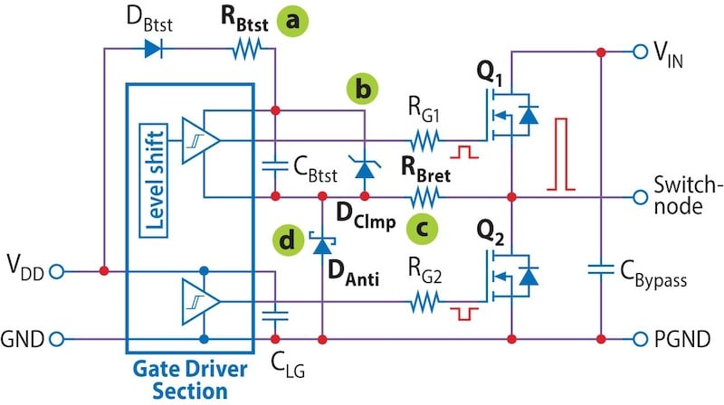
Figure 1(a-d). Recommended Si Gate driver augmentation for GaN FET compatibility. Image used courtesy of Bodo’s Power Systems [PDF]
4. Reverse conduction clamp: An anti-parallel Schottky diode across the low side of a half-bridge topology, as shown in Figure 1(d), can limit the magnitude of the negative switch node voltage the driver is exposed to. Some gate drivers become sensitive to or may even fail when the switch node falls below certain voltages below the ground reference. The voltage rating of this diode should match that of the low-side GaN FET. The current rating can be significantly lower than the low-side FET because it only conducts during dead times, so it should be selected based on its pulsed current rating.
Controller ICs and Integrated Gate Drivers
Controller ICs integrate many functions into a single IC, including the gate driver. Some of these ICs may not allow an optimal layout for GaN devices, so it is important to understand the design compromises to achieve the best performance.
When designing a power stage using GaN FETs, it is important always to follow the general layout recommendations. The order of consideration remains common-source-inductance (CSI), followed by the power and gate loop inductance. This means the power stage is essentially designed as a block, and the gate signals are connected to the controller IC, as shown in Figure 3. Variations of the recommended layout for the power stage block make it easier to choose an optimal block that can fit the controller IC. In the case of 2-phase controllers, choosing between two alternative designs may be necessary. The design criteria are to prioritize the control FET (switch), which is typically hard-switched, over the synchronous rectifier. For example, in a buck converter, the layout should be optimized to minimize parasitic inductance in the gate loop of the high-side FET. The same would be true for the low-side FET in a boost converter, as shown in Figure 3.
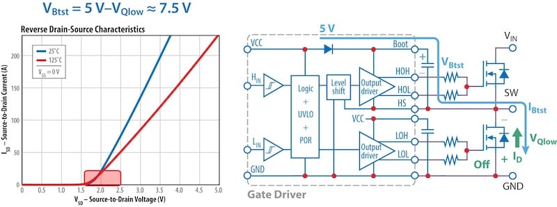
Figure 2. Bootstrap charging path during dead time. Image used courtesy of Bodo’s Power Systems [PDF]

Figure 3. Recommended layouts. Image used courtesy of Bodo’s Power Systems [PDF]
Adapting MOSFET Gate Drivers for Use with GaN FETs
To adapt MOSFET gate drivers for use with GaN FETs, designers must ensure compatibility, implement recommended modifications, and optimize layouts to harness the full potential of GaN technology. With careful attention to these guidelines, designers can use generic gate drivers and controllers, paving the way for successful high-volume production of GaN-based power converters.
This article originally appeared in Bodo’s Power Systems [PDF] magazine.