Facebook
 Google
 GitHub
 Linkedin
SiC, GaN, MOSFETs and More: PCIM 2024 Is a Wrap
This is the first in a two-part round-up reviewing the innovations announced at PCIM 2024. EEPower was onsite to learn about the latest power electronics progress.
More than 620 exhibitors introduced dozens of new products during the three-day 2024 Power Conversion and Intelligent Motion (PCIM) conference in Nuremberg, Germany, June 11-13. Their exhibits showcased innovations, developments, and trends in power electronics.
EEPower was onsite to learn the latest.
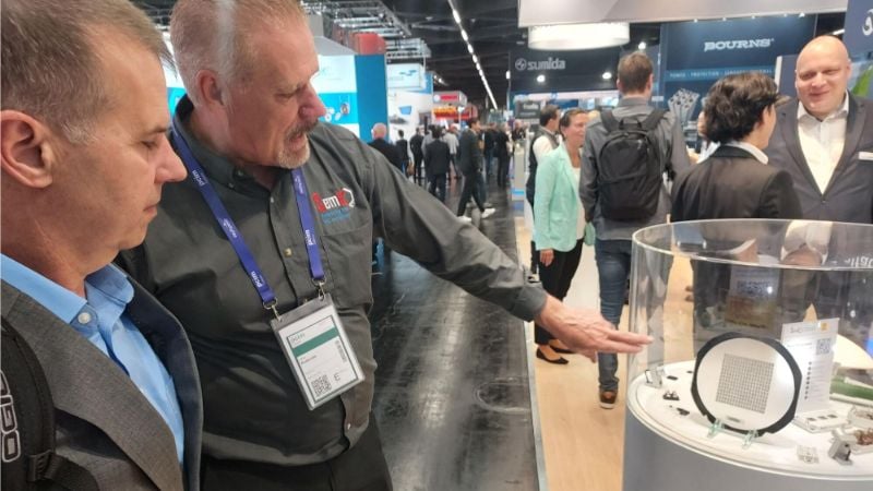
SemiQ speaks with EEPower’s Dale Wilson, director of engineering and content. Image used courtesy of EEPower
Cambridge GaN Devices: Power IC Packages
Cambridge GaN Devices (CGD) has launched two gallium nitride (GaN) power IC packages for the company’s ICeGaN family of GaN power ICs for data centers, inverters, and more.
GaN-based power devices offer several advantages over silicon-based devices. These include higher breakdown voltage, lower on-resistance, faster switching speeds, and better thermal conductivity. In addition, GaN provides smaller form factors, lower switching losses, and wider bandgap operation, enabling more efficient, compact, and high-frequency power conversion solutions across various applications.
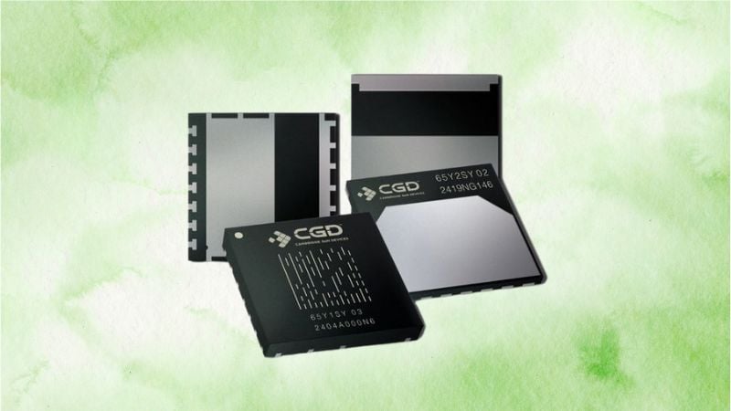
GaN power IC packages. Image used courtesy of CGD
GaN DFN (gallium nitride dual flat no-lead) is a surface-mount semiconductor package used for GaN power devices, specifically GaN power transistors or GaN FETs (field effect transistors). DFN-style packages are extremely rugged and reliable.
Developed for CGD, the DHDFN-9-1 (dual heat-spreader DFN) is a slim package with dual-side cooling and a compact 10x10 mm footprint, featuring wettable flanks to ease optical inspection. It boasts low thermal resistance and supports bottom-side, top-side, and dual-side cooling. It provides design flexibility and superior performance than the commonly used TOLT package, particularly in top-side and dual-side cooled setups. The DHDFN-9-1 package is engineered with a dual-gate pinout for optimal PCB layout and straightforward paralleling, making it ideal for applications up to 6 kW.
The two new packages are integral to CGD’s strategy to operate ICeGaN GaN power ICs at higher power levels. Servers, data centers, inverters/motor drives, micro-inverters, and other industrial applications increasingly benefit from GaN technology’s power density and efficiency. However, these applications also demand greater robustness, reliability, and integration ease. These new packages complement and enhance ICeGaN’s inherent attributes to meet these critical requirements, delivering increased power output, simplifying inspection, saving system cost, and improving reliability.
In addition, at PCIM 2024, CGD announced a series of Power GaN ICs designed to help customers and partners achieve and exceed a power density of 100 kW per rack in data centers. These devices align with recent high-density computing thermal design power trends. In motor control inverters, GaN technology reduces heat and creates more compact, durable power systems. CGD is aggressively targeting these markets with the high-power ICeGaN ICs. The P2 series ICs offer simplified gate driver design, reduced system costs, and advanced high-performance packaging, making them an excellent choice for these applications.
Alpha & Omega Semiconductor: SiC MOSFET Package Options
Alpha & Omega Semiconductor Limited (AOS) used PCIM 2024 to introduce its expanded surface mount and module package options for its 1200 V SiC MOSFETs. Based in Sunnyvale, California, the company designs, develops, and supplies power devices, wide bandgap power devices, power management ICs, and modules.
The first new surface mount package is available for the AOBB040V120X2Q, AOS’s latest 1200 V/40 mOhm αSiC MOSFET, housed in a standard D2PAK-7L surface mount package. This AEC-Q101-qualified product is designed to replace traditional through-hole packages. It is ideal for applications like electric vehicle (EV) onboard chargers, where efficient cooling can be achieved through vias and backside PCB heatsinks. This design simplifies assembly flow and maximizes power density. Additionally, the low-inductance package, combined with the fast driver source-sense connection, positions AOS αSiC MOSFETs among the most efficient power-switching solutions available.

Package options for 1200 V SiC MOSFETs. Image used courtesy of Alpha & Omega
AOS introduced the GTPAK surface mount package with topside cooling features for enhanced design flexibility. In applications where a topside-mounted heatsink is feasible, the direct heat path from the GTPAK minimizes thermal resistance, allowing higher power dissipation and more effective PCB routing. The first AOS product in the GTPAK is the AOGT020V120X2, a 1200 V/20 mOhm αSiC MOSFET, ideal for high-efficiency solar inverter and industrial power supply applications.
Finally, AOS announced the AOH010V120AM2, the inaugural product in its new AlphaModule high-power baseplate-less module family. This 1200 V/10 mOhm half-bridge αSiC module features press-fit pins and an integrated thermistor packaged in a standard footprint module. This design replaces multiple discrete devices with a single compact form factor, simplifying mechanical and electrical design by separating electrical and cooling paths. Single modules are suitable for residential solar inverters, while multiple modules in parallel can scale to the power levels required for fast DC charging stations.
With the continued growth in EVs, energy infrastructure, and renewable energy, there is increased interest in SiC MOSFETs. AOS says these new advanced package options will provide design flexibility to push power systems to higher density and efficiency.
SemiQ: Die Screening Program
Lake Forest, California-based SemiQ, a designer, developer, and global supplier of SiC solutions for ultra-efficient, high-performance, high-voltage applications, has launched a known-good-die (KGD) screening program. This program delivers high-quality, electrically sorted, and optically inspected SiC MOSFET technology, ready for back-end processing and direct die attachment.
SemiQ highlighted the screening program launched last month and is already operational at the PCIM 2024 event. The KGD ensures consistent electrical parameters, providing customers with repeatable performance and high end-of-line yield for equipment such as high-voltage supplies, traction inverters, and power conditioning systems. The uniform die parameters also facilitate the integration of multiple devices in high-power modules, enhancing productivity and delivering predictable, repeatable performance in high-efficiency applications.
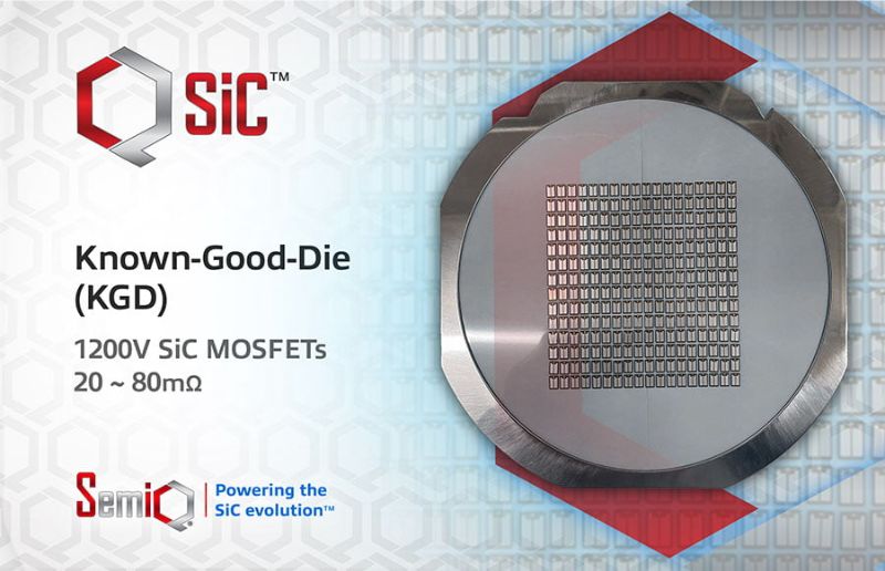
Known-Good-Die. Image used courtesy of SemiQ
The KGD program covers the complete portfolio of SemiQ’s QSiC 1200 V SiC MOSFETs, ranging from 20mΩ to 80mΩ. These products support electrification across automotive, e-mobility, renewable energy, industrial power, and other applications. With over a decade of experience, SemiQ has provided solutions in various fields, including solar energy, EV charging, automotive, medical, and energy storage.
SemiQ also introduced a compact and robust low-loss 1700 V SiC Schottky diode for solar inverters, switch mode power supplies, DC/DC converters, and EV charging. The GP3D050B170X (bare die) and GP3D050B170B (TO-247-2L package) diodes are rated for maximum forward currents of 110A and 151A (respectively). The devices’ design supports parallel configurations, enhancing flexibility and scalability in various power applications. The GHXS050B170S-D3 and GHXS100B170S-D3 dual diode packs are rugged modules supplied in a SOT-227 package, providing easy reliability and efficiency.
Mitsubishi Electric: IGBT Modules
Mitsubishi Electric has unveiled its latest (8th generation) LV100 IGBT modules at PCIM 2024. The LV100 supports many high-power applications, including photovoltaic systems, energy storage, wind power, and industrial drives.

LV100 with 8th Gen IGBT 1200 V/1800 A. Image used courtesy of Mitsubishi Electric
The 8th generation 1.2k V/1800 A LV100 module is still under development, but it will achieve a significant upgrade over the existing 1200 A maximum current rating, which will now expand to 1800 A with advanced IGBT and diode chipsets. This makes it suitable for various applications, including photovoltaic and battery energy storage systems.
For lower-voltage applications, Mitsubishi Electric is developing a series of 2.5 kV LV100 power modules designed to enhance reliability by optimizing the voltage rating for improved performance in 1000 VAC applications.
Navitas Semiconductor: SiC MOSFETS
Just ahead of PCIM 2024, Torrance, California-based Navitas Semiconductor announced its Gen-3 Fast (G3F) 650 V and 1200 V SiC MOSFETs portfolio. The G3F family has been optimized for high-speed switching performance, resulting in a 40% improvement to hard-switching figures-of-merits compared to the competition in continuous conduction mode totem-pole power factor correction systems used in power supply units for applications such as EVs, solar power, battery electric storage systems, and high-power computing systems. In one such application, the G3F allows the next-generation AI PSUs' wattage to increase up to 10 kW and the power per rack to increase from 30 kW to 100-120 kW—up to three times more power.
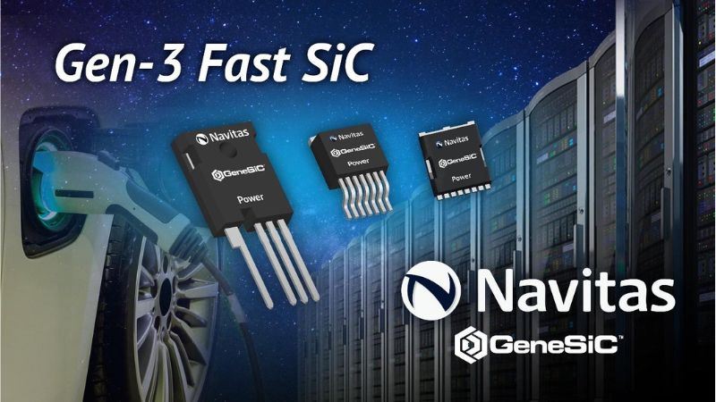
Gen-3 Fast SiC. Image used courtesy of Navitas
According to Navitas, The G3F GeneSiC MOSFETs are crafted using a proprietary trench-assisted planar technology. These MOSFETs surpass traditional trench MOSFETs in performance while offering superior robustness, manufacturability, and cost-efficiency compared to competitors. They deliver high-efficiency and high-speed performance, achieving up to 25°C lower case temperatures and up to three times the lifespan of competing SiC products.
The trench-assisted planar technology ensures an extremely low RDS(ON) increase with temperature, leading to the lowest power losses across the entire operating range. This offers up to 20 percent lower RDS(ON) in real-life high-temperature operations than the competition.
Furthermore, all GeneSiC MOSFETs boast the highest-published and 100 percent-tested avalanche capability, a 30 percent longer short-circuit withstand time, and precise threshold voltage distributions for easy paralleling. These features make GeneSiC MOSFETs an ideal choice for high-power, fast-to-market applications.