Facebook
 Google
 GitHub
 Linkedin
A Closer Look at Modular Silicon Carbide Device Evaluation
In this article, we deep-dive into modular design evaluation, how the modular design concept works, and how to reap its benefits.
This article is published by EEPower as part of an exclusive digital content partnership with Bodo’s Power Systems.
The high-performance capabilities of silicon carbide (SiC) are changing the landscape of power electronics, bringing with it benefits such as superior efficiency, increased power density, and enhanced thermal performance. Notably, automotive applications are benefiting significantly from SiC technology, using it primarily for main propulsion, onboard chargers, and battery-charging stations.
SiC’s dielectric strength, ten times that of silicon, enables the creation of high-voltage devices that meet the demands of charging infrastructures and smart grids. Moreover, the high switching frequency of SiC allows for reducing the physical size of components like magnets and inductors.

Image used courtesy of Adobe Stock
This, however, is just the tip of the iceberg. SiC power devices are making their mark in diverse applications, from power supplies and BEV power conversion for battery charging and traction drives to industrial motor drives and renewable-energy-generation systems such as solar and wind power inverters.
However, making the best use of SiC requires changes in design approaches, often leading to substantial changes to the printed circuit board (PCB) and fewer secondary components such as coolers and transistors, which reduces cost and saves space. With that, design evaluation tools that accommodate these changes and enable swift, precise testing of new designs and careful assessment of device reliability are essential.
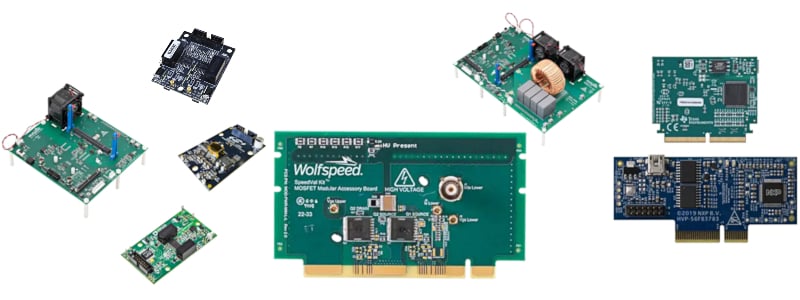
Figure 1. The platform consists of a motherboard, gate-driver card, power-daughter card, optional control card, and other potential accessories. Image used courtesy of Bodo’s Power Systems [PDF] and Wolfspeed
Ecosystem of Building Blocks: The Modular Design
Essentially, the modular design is a toolkit, providing an ecosystem of building blocks to streamline the process of SiC device evaluation. It facilitates rapid, comprehensive system-level testing across diverse SiC products in both surface-mount and through-hole packages. The core objective of this kit is to simplify and expedite the design process for engineers, designers, and manufacturers. It allows for concurrent testing and optimization of the MOSFET and the intended gate driver before the actual hardware design begins. The kit allows engineers to establish and evaluate the controller, gate driver, magnetics, and SiC devices for the power converter all in one go, instead of independently designing each system.
The evaluation platform is composed of a main circuit board, a power module, a gate driver module, and an optional control module, along with other potential add-ons. Designers can test a variety of discrete devices up to 1,200 V in combination with a range of gate-driver options from various manufacturers, using a “drop-in” approach. To be effective, such platforms should accommodate a broad spectrum of voltages, packaging styles, and power topologies, making them adaptable for most applications. This allows setting parameters for various testing modes like double-pulse or buck- or boost-power testing via a computer-based graphical user interface, eliminating the need for external function generators or controllers for PWM generation. With this, firmware engineers can start developing and testing custom firmware needed for their product on a real high-voltage/high-power design as opposed to merely a low-voltage controller development board. Let’s take a closer look at the individual components.
The Motherboard
The motherboard in our example (Figure 2) has a low-inductance layout and features screw-terminal power connections, accommodating the efficient testing of SiC devices. The power-daughter cards, tailored for each device package, employ coaxial connectors for VGS and VDS measurements, thereby ensuring optimal signal integrity. They also use high-bandwidth current sensing for precise switching-loss measurements. The modular design of the power daughter cards allows the platform to evaluate a range of SiC devices, from surface-mount TOLL devices to TO-247 packages. It can be expected that modular design plans extend beyond the initially introduced half-bridge motherboard, with versions such as a three-phase variant for inverters and motor control in the pipeline.
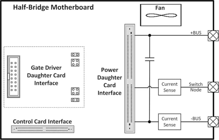
Figure 2. Half-bridge motherboard layout. Image used courtesy of Bodo’s Power Systems [PDF] and Wolfspeed
The central board is fundamentally set in a half-bridge configuration. It features slots for the gate driver card, the power daughter card, and an optional control card. Further, it incorporates a cooling fan, film, and ceramic DC bus capacitors, along with external power and signal connections. Current and voltage sensing is also a part of its design.
MOSFET and Gate Driver Test - Before the Onset of Hardware Design
The customized daughter-card gate-driver boards have been developed by industry-leading gate-driver companies in conjunction with Wolfspeed and can facilitate comprehensive testing of the entire range of SiC MOSFETs. The gate driver cards serve a critical function in the analysis and optimization of SiC devices. Designing with SiC MOSFETs often brings unique challenges related to parasitic inductance and capacitance in the layout due to high dV/dt and di/dt. Additionally, the gate driver can influence the SiC MOSFET’s switching performance.
Analyzing the entire gate circuit is key to de-risk the design processes. Each gate-driver card carries two isolated gate-drive outputs and corresponding isolated bias supplies to drive the half-bridge power-daughter card. In applications where short-circuit protection is required, several of the gate driver cards available in the platform include this feature. This allows for optimizing the response time and validating the performance on the evaluation board prior to starting the final design.
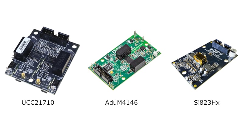
Figure 3. Gate driver cards Si823Hx by Skyworks, AduM4146 by Analog Devices, and UCC21710 by Wolfspeed, are all compatible with this modular evaluation kit. Image used courtesy of Bodo’s Power Systems [PDF] and Wolfspeed
The gate driver cards (Figure 3) within the evaluation platform are instrumental in analyzing the performance of SiC devices. They provide a means for engineers to measure important factors like QRR and switching loss (EON, EOFF, ERR), contributing to an understanding of the device’s operational efficiency. Timing metrics such as TDELAY-ON, TDELAY-OFF, TRISE, and TFALL can also be determined, giving an overview of the device’s performance under different conditions. The gate resistance can be tuned to provide the ideal balance of switching losses and dV/dt or VDS voltage overshoot based on the operating conditions of the application.
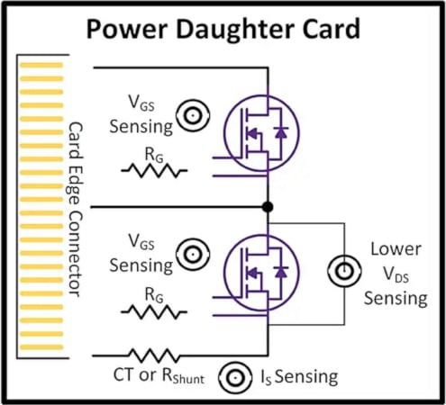
Figure 4. Power daughter card layout and features. Image used courtesy of Bodo’s Power Systems [PDF] and Wolfspeed
Power-Daughter Cards: Testing a Wide Range of SiC MOSFETs
The power-daughter card (Figure 4) in the evaluation platform is set up as a half-bridge. Each card includes the high-side and low-side SiC MOSFET, and high-bandwidth current sensing using either a shunt or CT. They can be configured for operation in a double pulse test with high-fidelity current measurement, or to run in a continuous power buck or boost converter with forced air cooling. Engineers have the freedom to use their preferred gate driver and feature set to test devices on the cards, taking measurements, and refining the performance of the SiC MOSFET and gate-driver pair. In addition, SiC devices can be substituted by switching the power-daughter card, avoiding soldering, and maintaining a low-inductance connection to the DC bus for optimal switching performance. Power daughter cards are available for TOLL, TO-263, and TO-247 MOSFETs, allowing the user to evaluate different packages, voltage ratings, and RDS(ON) devices within a single platform. With SiC as a proven solution for 1,200 V applications, an area where lateral GaN technology faces challenges, these provisions for testing are particularly beneficial.
High-Power Thermal Testing Under Real Operating Conditions
In the evaluation kit used here as an example, gate resistance (RG) can be adjusted to optimize switching behavior and assess discrete SiC MOSFETs up to 1,200 V across various package types. These assessments can be done within preferred topologies like a buck or boost converters using a half-bridge motherboard. This platform also enables high-power thermal testing under real operating conditions. A comprehensive modular SPICE model accompanies the hardware testing, allowing engineers to compare test results with simulations, aiding the development of their designs.
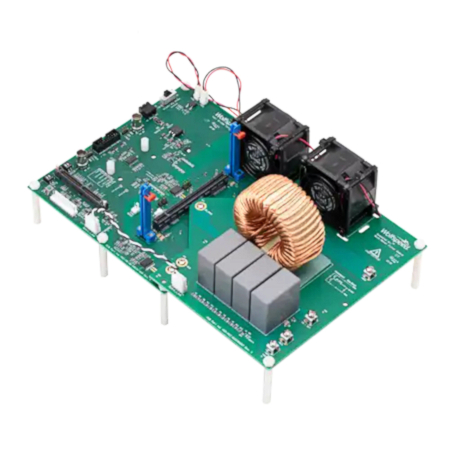
Figure 5a. Buck-boost board. Image used courtesy of Bodo’s Power Systems [PDF] and Wolfspeed
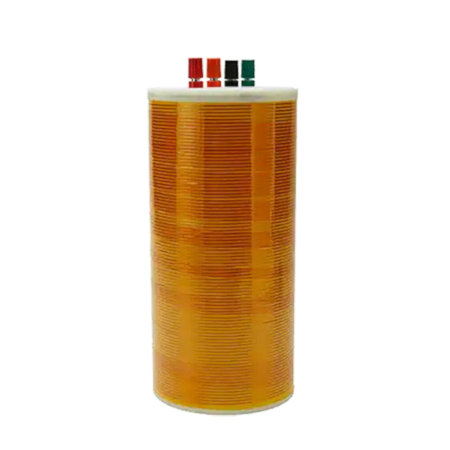
Figure 5b. Air core inductor. Image used courtesy of Bodo’s Power Systems [PDF] and Wolfspeed
Additionally, the SPICE system model provides estimates of key parasitic elements. This not only enhances the simulation’s accuracy but also guides engineers in controlling these elements, a critical aspect when working with SiC MOSFETs. Lastly, an optional buck-boost board is available, allowing application-specific testing at different power levels. A custom-designed air-core inductor (figure 5b) offers options to minimize parasitic capacitance, ensuring accurate double pulse testing (DPT), crucial for optimizing buck or boost converter designs.
With the buck-boost filter boards (5a), a buck or boost converter application can be run at full power on this kit. This allows thermal data as well as converter efficiency to be measured (figure 6).

Image used courtesy of Bodo’s Power Systems [PDF]

Figure 6. Example measurements made on a 20 kHz synchronous boost converter running with thermal image at 16.5 kW. Image used courtesy of Bodo’s Power Systems [PDF] and Wolfspeed
SiC Device Evaluation Takeaways
With the increased demand for energy-efficient conversion at the highest power density in many industries, from electric vehicles to solar power and data centers, the importance of SiC device evaluation will continue to grow in power electronics. In this context, power device testing extends beyond just the datasheet parameters. With modular SiC device evaluation using the SpeedVal Kit platform, engineers can accelerate their design cycle by performing critical testing without the time-consuming and costly hassle of building totally new designs for each test. Furthermore, all of the design files for the SpeedVal Kit are available, allowing engineers to reuse pieces of the platform in their own design, reducing design risk.
By offering a comprehensive solution, modular design evaluation enables full power validation through the inclusion of all necessary components, including the gate driver and control boards. It allows for testing before hardware is on-set, within different voltage ranges, and simplifies the process of accurate switching measurements with its low inductance power loop and current sense design. Importantly, the modular nature of SiC test kits like the SpeedVal Kit allows for the selection of different boards to customize test conditions according to specific application requirements.
As the industry strives for improved efficiency, smaller size, lower weight, and cooler designs, the application of SiC components will continue to grow. To this end, the modular approach to SiC device evaluation is an effective strategy to achieve an optimized design, offering a promising role in the future of power electronics.
This article is co-authored by Johannes Kemper, field application engineer, automotive, and Adam Anders, manager of power platforms with Wolfspeed. The article originally appeared in Bodo’s Power Systems [PDF] magazine.