Facebook
 Google
 GitHub
 Linkedin
SiC MOSFET Modules for PV Systems With Integrated Storage, EV Charging
This article discusses how SIC-MOSFETs in innovative packages can enable novel converter concepts to support ever-increasing efficiency and power density requirements.
Decarbonization trends are driving a transition in every layer of the energy sector. In the residential sector, examples are the adoption of e-mobility, solar energy, and home energy storage.
The world is facing challenges due to the consequences of using fossil fuel energy sources. To address these challenges, the energy sector is under transition. Transitions occur not only on the generation side of electric energy with a shift towards using more renewable energy sources but also in the way that energy is utilized in the different sectors. Examples of transitions that directly impact electricity consumption in the residential sector are the increased adoption of electric vehicles, including plug-in hybrids as well as the shift to electric heating with heat pumps. The change in electricity utilization and increasing cost for residential electricity results in increased adoption of residential solar photovoltaics, home electricity storage, and EV charging at home. This article discusses how SiC MOSFETs in innovative packages can benefit the realization of a power electronic converter concept that integrates demands for photovoltaics, energy storage, and EV charging in an efficient manner.
Many households today already make use of solar photovoltaic (PV) systems. Systems without local energy storage feed the available power into the electricity grid if it is not immediately needed to supply local loads. The remuneration for electricity fed back into the grid is, in most cases, much lower than the cost of electricity purchased from the grid. Therefore, the PV system operator has an interest in maximizing the consumption of electricity obtained from PV and minimizing the purchase of energy from the grid. This can be achieved with a local energy storage system (ESS) and, in principle, two approaches can be followed for adding an ESS to a PV system.
AC-coupled energy storage systems can be added to existing PV installations that already have an existing PV inverter without an integrated storage option. Here, the energy that gets stored and used later passes multiple stages of conversion, as illustrated in Figure 1 a). In this kind of system, energy stored for later usage passes through four conversion stages during the storage phase and again through two stages when it is provided to the local loads. Even assuming 98% efficiency for each stage, this results in an overall conversion path efficiency of 88.5%.
New installations for PV systems that include an energy storage option will most likely make use of a PV inverter that has an integrated power stage to couple the energy storage to the DC bus. This approach reduces the amount of power conversions between electricity generation, storage, and water consumption, as shown in Figure 1 b). Here only two stages are passed in the storage phase and another two in the utilization phase of the stored energy from the battery. This reduction of conversion steps results in an increased efficiency of 92%, assuming again 98% efficiency of each conversion stage.
In addition to the energy storage in residential PV installations, more and more charging points for electric vehicles (EVs) are also being installed in peoples’ homes now. This so-called home charging can be realized in two different ways: AC charging or DC charging. The most common approach today is AC charging. Here, an AC wallbox provides AC to the electric vehicle, which is then converted through the onboard charger (OBC) into DC and applied to the vehicle battery. The alternative is to install a so-called DC wallbox that handles the conversion of AC to DC, which is then provided to the vehicle. Both approaches are illustrated in Figure 2. From an energy flow perspective, these are very similar both for the case of providing PV energy directly to the vehicle for charging and for the case of transferring stored energy from the ESS to the EV battery. The main difference is whether the power conversion for EV charging is done inside or outside the vehicle.

a) PV and ESS with AC-coupling. Image used courtesy of Bodo’s Power Systems [PDF]

b) PV and ESS with DC-coupling
Figure 1. Photovoltaic systems with local energy storage. Image used courtesy of Bodo’s Power Systems [PDF]
As a logical step of integration and optimization, the function of the DC wallbox can be integrated into the PV inverter with (or without) an energy storage option. The resulting integrated converter concept is illustrated in Figure 3. By coupling the ESS and EV charging with the PV inverter at the common DC link, it is possible to shift energy from any input port to any output port by just using just two conversion stages. This reduction of conversion stages results in an increased efficiency of 96% between every two nodes, assuming again 98% efficiency of each conversion stage. Of course, if the energy generated by the PV is firstly stored in ESS and then used for charging or local loads, an efficiency of 92 % is expected. If the EV and the isolated DC/DC converter support bi-directional operation, the EV battery can even be used as additional local storage while a vehicle is connected.

a) PV with ESS and AC wallbox. Image used courtesy of Bodo’s Power Systems [PDF]

b) PV with ESS and DC wallbox
Figure 2. PV with ESS and additional wallbox for EV charging. Image used courtesy of Bodo’s Power Systems [PDF]
In addition to enabling improvements in power transfer efficiency, the integrated system also offers possibilities for reduced investment costs. The single integrated converter discussed here contains one less conversion stage than a solution with a PV inverter with ESS and a separate DC wallbox and only one housing is needed. Thus, the cost of a converter like this can be expected to be less than that of two separate units.
To realize this integrated converter, four power conversion stages are required. Some topologies options are discussed in the next section, and suggestions on how to implement them with small power electronics modules containing the latest generation of ROHM SiC MOSFETs are presented. The modules considered here are taken from the upcoming line-up for compact transfer molded packages containing SiC Gen 4 SiC MOSFETs shown in Table 1.

Figure 3. PV inverter with integrated ESS and DC charging for EV. Image used courtesy of Bodo’s Power Systems [PDF]
Table 1. Planned line-up of compact modules with SiC Gen 4 MOSFETs (subject to change). Image used courtesy of Bodo’s Power Systems [PDF]


Figure 4. Uni-directional Boost converter. Image used courtesy of Bodo’s Power Systems [PDF]

Figure 5. Bi-directional DC/DC converter. Image used courtesy of Bodo’s Power Systems [PDF]
For the discussion in this article, a nominal power rating in the range of 11 kW is assumed, which is expected to be in the power range of most residential PV systems. As a system of this power range is interfacing to the grid with a three-phase connection, the DC link voltage is around 800V, mandating the use of 1200V semiconductors. In this voltage region, SiC MOSFETs can provide significant benefits over Si IGBTs in terms of performance. For the DC/DC stage interfacing the PV modules to the common DC link, the simplest possible solution is a standard boost converter, as shown in Figure 4. In the typical power range considered here, it is quite common to realize this using multiple such boost converters operating in parallel to provide independent maximum power point tracking for multiple PV strings. The interface to the high-voltage battery can be realized as a bidirectional DC/DC converter, as illustrated in Figure 5.
The DC/AC stage needs to be realized using a bi-directional circuit to enable power flow to the grid/local AC loads as well as power flow from AC to DC to charge the EV during times when the local storage battery is empty and no energy from PV is available. A topology that can meet these requirements with minimal effort and – using SiC MOSFETs – with high efficiency is the three-phase full-bridge illustrated in Figure 4.

Figure 6. Three-phase full-bridge for DC/AC stage. Image used courtesy of Bodo’s Power Systems [PDF]
The DC/DC stage for the EV charging port is usually implemented as an isolated converter for safety. The common DC link in the integrated power converter is fixed at around 800V. The DC/DC converter output needs to cover a wide voltage range to support EVs with battery voltages of around 400V as well as those with batteries in the 800V range. Therefore, the use of a CLLC topology, which is quite common in OBCs, is not advisable here, as it is not optimal in situations where the input-to-output transfer ratio is changing across a wide range. Instead, a dual-active bridge (DAB), as shown in Figure 7, is preferable.

Figure 7. Dual active bridge (DAB). Image used courtesy of Bodo’s Power Systems [PDF]
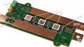
All the topologies shown here can be realized using 1200V SiC MOSFETs (and SBDs for the boost stage) in discrete packages (e.g., TO247-4L). As illustrated in Table 2, a realization using only discrete components will require a total of 24 power semiconductor devices. For a discrete solution, the creepage requirements must be addressed on the package level for each transistor switch. This results in rather large components, even if the SiC dies inside the package are small. By combining multiple dies inside a single transfer molded package, the overall space requirement is reduced – in part due to the fact that creepage can be addressed once for an entire topology. In Figure 8, this is illustrated for a six-switch full-bridge module.

Figure 8. Combining the function of six TO-247-4L in one HSDIP module saves space. Image used courtesy of Bodo’s Power Systems [PDF]
The switching loss performance of BST38T2P4K01-VW (36 mΩ, 1200 V, 6 in 1) was evaluated in a test board realizing an AC/DC stage for an OBC application [1]. The results of the switching loss evaluation through double pulse tests of this module, shown in Figure 9 a), are equally applicable to the case of a bidirectional DC/AC stage considered here. Based on this data, a simulation of a bidirectional AC/DC stage for an 11 kW system was performed. The simulation results shown in Figure 9 b) predict that an 11 kW AC/DC stage based on BST38T2P4K01-VW will have an efficiency of around 99%, assuming a switching frequency of 48 kHz and the use of a heatsink with forced air cooling considering only semiconductor losses.

a) Experimentally determined switching loss [1]. Image used courtesy of Bodo’s Power Systems [PDF]

b) Simulated efficiency AC/DC and DC/AC operation (fSW = 48 kHz).
Figure 9. Switching loss and simulated efficiency of BST38T2P4K01-VW (36 mΩ, 1200 V, 6 in 1). Image used courtesy of Bodo’s Power Systems [PDF]
Not just the full-bridge for the DC/AC stage of the integrated PV inverter with local storage and EV charging additions can be realized with such a small transfer molded package. Also, the various DC/ DC stages can be addressed with different types of modules from the line-up shown in Table 2. For the multi-MPPT boost, the three half-bridges of a 6 in 1 module can be used, and the DAB can be built using two 4 in 1 modules. The non-isolated DC/DC converter can be designed in multiple ways, using either a multi-phase DC/DC approach with interleaving based on a 4 in 1 or 6 in 1 module or by utilizing the half-bridge modules.
Table 2. Quantities of semiconductor components
| Converter Stage | Discrete Components | Module |
| Boost (PV MPPT) | 6 (assuming 3x MPPT) | 1 (6 in 1) |
| DC/DC (battery interface) | 4 (paralleling) | 1 (2 in 1) |
| DC/AC (bi-directional) | 6 | 1 (6 in 1) |
| DC/DC (EV charging) | 8 | 2 (4 in 1) |
| Total: | 24 | 5 |
Both module types in Table 2 meet industry standards for robustness and reliability and were specifically developed to provide an optimal solution for compact converter designs. These modules are targeting not only the application of integrated PV inverters with storage and EV charging options discussed here but additionally can be valuable building blocks also for other industrial or automotive applications.
Additionally, to BOM size reduction, the proposed modules reduce the size of the required PCB and heatsink area. Simulation models for PLECS and datasheets are also available.
Conclusion SiC MOSFET Modules as Efficient Building Blocks
The article described SiC MOSFET modules as efficient building blocks for power electronic converters that integrate demands for photovoltaics, energy storage, and electric vehicle charging. It discussed the benefits of integrating energy storage and EV charging with PV systems and compares the efficiency of AC-coupled and DC-coupled energy storage systems.
The integrated system not only improves power transfer efficiency but also offers possibilities for reduced investment costs. Overall, the use of 1200 V SiC MOSFETs in these innovative packages can benefit the realization of efficient power electronic converter concepts for PV systems with integrated storage and EV charging.
[1] M. Jankovic, I. Fouaide, M. Hondo, H. Tan; Increasing the Power Density of Bidirectional On-Board Chargers with a New Silicon Carbide Power Module, PCIM Europe 2023
This article originally appeared in Bodo’s Power Systems [PDF] magazine and was co-authored by C. Felgemacher, M. Albayrak, M. Jankovic, C. Fuentes, and J. Hueskens of ROHM Semiconductor.
Featured image used courtesy of Adobe Stock