Facebook
 Google
 GitHub
 Linkedin
IGCT Platform for up to 8.5 kV and Advanced Turn-Off Current Capability
Learn how Hitachi Energy's IGCT platform scales to 8.5 kV. It provides high turn-off capability and supports cost-efficient system designs for HVDC and wind power.
Article co-authored by Hitachi Energy’s Umamaheswara Vemulapati, Urban Meier, Mark Frecker, Thomas Stiasny, Christian Winter, and Zuzana Ptakova.
This article is published by EEPower as part of an exclusive digital content partnership with Bodo’s Power Systems.
High power semiconductor applications are more and more evolving into higher power ratings. At the same time, there is increasing pressure on cost. High-voltage IGCT enables the design of these applications to be significantly more cost-efficient, e.g., by reducing the number of series-connected cells in a MMC topology. The new platform applies the latest technologies, which result in unprecedented turn-off capability at high voltage ratings up to 8.5 kV. On top, the IGCT circuit offers advantages with respect to converter protection, e.g., fault current limitation, SCFM, and case rupture.
Power semiconductors are used in many demanding high-power applications like HVDC, Medium Voltage Drives, offshore wind turbines, or rail-interties. For these applications, the trend goes towards higher voltage and current ratings. The new IGCT platform with voltage ratings up to 8.5 kV and outstanding thermal and dynamic behavior, addresses these demanding requirements. Thanks to the robust and hermetic housing, the IGCT is ready to deal with demanding protection requirements.

Image used courtesy of Adobe Stock
IGCT Power Handling Scalability
The IGCT is a mature component used in demanding applications like industrial motor drives, offshore wind turbines, and rail supply, all of which demand the highest availability, efficiency, and power handling scalability. IGCT technology is evolving to support higher power applications with elevated current and voltage ratings.
The IGCT device currently used in the majority of the applications in the field is the L-type, Reverse conducting (RC) or Asymmetric (AS) IGCT with an 85 mm diameter pole piece and 4.5kV or 6.5 kV blocking voltage. Smaller power requirements can be met with RC IGCT devices. To enhance power handling capabilities, an AS IGCT with a discrete antiparallel freewheeling diode or increased device area can be employed.
Addressing applications with the highest power demand, devices with increased area are required. Hitachi Energy is developing a device platform with a pole piece diameter of 138 mm. The development activities focus on high-voltage devices with 6.5 and 8.5 kV blocking capability. High-voltage devices offer some advantages, particularly for applications using multilevel topologies.
These applications can be designed with a reduced number of series-connected multilevel cells and consequently reduced cost by applying HV IGCT devices. Table 1 provides the RMS and turn-off current capability overview for Hitachi Energy’s 85 mm and 138 mm IGCT platforms.
Table 1. Overview of selected IGCT types with 85 mm and 138 mm pole piece diameter
|
Pole piece diam. (mm) |
Blocking voltage I DClink (kV) |
Status |
Type |
IT(RMS)*) (A) |
Turn-off capability (A) |
|
85 |
4.5 / 2.8 |
product |
RC |
2010 |
3,600 |
|
85 |
4.5 / 2.8 |
product |
AS |
4340 |
6,500 |
|
85 |
6.5 / 4.0 |
product |
RC |
1600 |
2,600 |
|
85 |
6.5 / 4.0 |
product |
AS |
3000 |
4,400 |
|
138 |
6.5 / 4.0 |
prototype |
RC |
3700 |
8,000 |
|
138 |
6.5 I 4.0 |
prototype |
AS |
6300 |
12,000 |
|
85 |
8.5 / 5.0 |
prototype |
RC |
1250 |
2,000 |
|
85 |
8.5 / 5.0 |
prototype |
AS |
2042 |
3,000 |
|
138 |
8.5 / 5.0 |
prototype |
RC |
3000 |
5,500 |
|
138 |
8.5 / 5.0 |
prototype |
AS |
4550 |
10,000 |
*) IT(RMS): RMS on-stat current at half sine wave, semiconductor case temperature 85 degC.
Device Design
An IGCT device is made up of three intimately meshing parts: semiconductor, housing, and gate unit. Scaling current handling capability with device area is a known challenge, see, for example, [5]. At present, the state of the art is manufacturing a single IGCT device on a 150 mm, “6 inch”, silicon wafer (see, for example, [1] through [4]). Accounting for loss of wafer real estate due to flats and notches, production margins and junction termination, approximately 150 cm2 remains available for active, cooled, device area.
Applying water cooling and reasonable pumping effort, the device area potentially represents massive power-handling capability, suitable for the highest power applications, even if the device area is shared with a free-wheeling diode alongside the IGCT switch in the Reverse-Conducting (RC-) IGCT. Here, results for an RC-IGCT with AGCT / ADiode ≈ 1.35 are presented. The choice of area ratio is ultimately a question for the customer, whose wishes will vary depending on the application. Testing of RC-IGCTs with different area ratios is planned.
The platform described here was improved over the one presented in 2014 [2]. The GCT segment layout of the switch part of the wafer was adapted to the state-of-the-art [6], and the diode has been fitted with a segmented cathode [7] for improved switching behavior. In addition, the platform’s performance at higher voltage has been improved by applying the high-voltage vertical design already presented for smaller device sizes [8]. To meet increased insulation requirements anticipated for the high voltage (≥ 6500 V) branches, the housing was increased to 35 mm.
In terms of scaling the controllable current, the AS poses the challenge due to the increase in the physical size of the gate circuit, which is an unavoidable consequence of the increase in the switch’s active area. To compensate for this, testing the maximal controllable current with an improved gate circuit is investigated.
Reverse Conducting (RC) 6.5 and 8.5 kV
Both the 6.5 and 8.5 kV RC-IGCT prototypes were tested beyond the requirements on maximal current controllability (MCC). The appreciation of MCC requirements originates in application simulations that indicate a Tvj-dominated performance limit rather than MCC. Figure 1 shows waveforms from both voltage classes, switching currents above the anticipated MCC ratings.
The corresponding loss trade-off curves are shown in Figure 2.
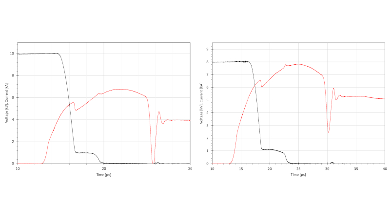
Figure 1. Illustration of probing the current controllability for the 6.5kV (left, 10000 A) and 8.5 kV (right, 8000 A) RC-IGCT prototypes. Image used courtesy of Bodo’s Power Systems [PDF]
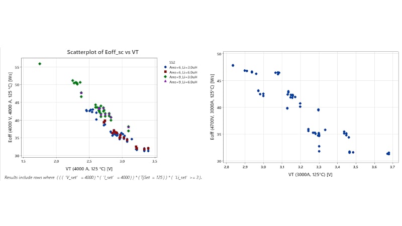
Figure 2. Trade-off between dynamic and static losses for the 6.5kV (left) and 8.5kV (right) GCT part of the RC-IGCT prototypes. Image used courtesy of Bodo’s Power Systems [PDF]
Outlook Asymmetric (AS) IGCT
It is sensible to strive for the maximum challenge during technology development. For this reason, the 4.5 kV and 6.5 kV voltage classes were selected for the first prototype series. It is expected that the current controllability limit will be dictated by either the gate circuit impedance or its current capability.
The aim is to verify significantly higher current controllability than 10 kA, ideally beyond 14 kA for the 4.5 kV AS-IGCT. Getting better information on which aspect of the device poses the limit is also a target for the test series on the AS-IGCT prototypes. However, as already mentioned above, at present, there are only results available at lower currents. Figure 3 shows such a sample waveform.
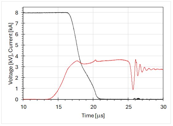
Figure 3. Illustration of the 4.5 kV AS-IGCT prototype switching 8 kA at 140°C for Eoff characterization. Image used courtesy of Bodo’s Power Systems [PDF]
Applications
Overview
IGCTs are used in high-power applications. As the IGCT is based on a Thyristor structure, the device can be tailored to the lowest on-state losses to be the perfect match for low-frequency applications, like DC breakers [9] or MMC topologies [10], concerning system losses.
The turn-on dI/dt control is achieved by a dI/dt choke in combination with a clamp circuit. This leads to a nearly full elimination of the turn-on losses in the IGCT. Additionally, the DI/di choke limits fault current peaks in case of device or system failures and can therefore prevent case ruptures and severe damage. Together with the SCFM capability of the press pack construction of the device package, the IGCTs offer significant advantages in application using the MMC topology.
Unpowered dV/dt Capability for Startup
The IGCT with a powered gate unit shows a remarkable dV/dt capability in the blocking state. During dV/dt events, the displacement current is extracted through the gate and the very low inductive gate path of the gate unit. This prevents latch-up of the thyristor structure, even with dV/dt above 10kV/ms.
In applications like MMC, auxiliary power for controllers and gate units is often generated out of the DC-link capacitor voltage. During system start-up, the auxiliary power is not available in the beginning until the capacitor is charged to a certain voltage.
With an unpowered gate unit, for dV/dt events, the displacement current extraction through the gate unit is not available. Here, the extraction of the displacement current is managed through anode shorts, as is also well-known from GTOs. In this regime, the dV/dt capability is significantly lower than for a powered gate unit. The dV/dt capability of 4.5kV and 6.5kV IGCTs without a gate unit is shown in Figure 4.
The dV/dt capability of an IGCT is strongly temperature dependent (lower temperature – higher dV/dt capability). During system startup, power semiconductors are at the cooling water temperature. As the voltage rise during system power-up is typically limited, the unpowered IGCT can easily cope with the period until the DC-link capacitor voltage is high enough to supply auxiliary power.
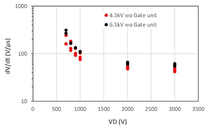
Figure 4. dV/dt capability at Tj = 60°C of a 4.5kV and a 6.5kV IGCT with an unpowered Gate unit. Image used courtesy of Bodo’s Power Systems [PDF]
Conclusion
- IGCT offers an excellent possibility to scale in voltage and area.
- Design for large-sized IGCTs for several voltage classes has been presented with unprecedented thermal and dynamic performance.
- Ideal for high-power applications like MMC, e.g., used in HVDC.
References
1. “6 kV 5 kA RCGCT with advanced gate drive unit”, Gruening et.al., Proc. ISPSD 2001, Osaka, Japan.
2. “The 150 mm RC-IGCT: a device for the highest power requirements”, Wikström et al., Proc. ISPSD 2014, Hawaii, U.S.A.
3. “New ultra high power reverse conducting GCT reaches 6kV/5kA”, Donion et.al., Proc. PCIM 2001, Nürnberg, Germany.
4. “450MVA STATCOM installation plan for stability improvement”, Akedani et.al., Proc. CIGRE 2020, Paris, France.
5. The corrugated p-base IGCT – a new benchmark for large area SOA scaling, Wikström, et.al., Proc. ISPSD 2007, Jeju Island, Korea.
6. “A 6500 A, 4500V, 94 mm Asymmetric[sic] IGCT”, Wikström, Cottet, Proc. PCIM 2020, Nürnberg, Germany.
7. A 4.5kV RC-IGCT with Diode Segmentation for MMC Inverters, Wikström et.al., Proc. PCIM 2022, Nürnberg, Germany.
8. Vemulapati et.al., “High-Voltage (8.5 kV) Asymmetric IGCT for MVD and HVDC Applications” in Proc. ICPE 2023 – ECCE Asia, Jeju Island, Korea.
9. “Semiconductor circuit-breaker based on RB-IGCT to protect LVDC microgrids”, Antoianzi, et.al., CIGRE Paris 2024
10. “Rugged MMC converter cell for high power applications” Oede - gard. et.al. EPE ECCE Europe 2016
This article originally appeared in Bodo’s Power Systems [PDF] magazine and is co-authored by Tobias Wikström, Hitachi ABB Power Grids; Umamaheswara Vemulapati, Urban Meier, Mark Frecker, Thomas Stiasny, Christian Winter, all Hitachi Energy, Semiconductors, Switzerland; and Zuzana Ptakova, Hitachi Energy, Semiconductors, Czech Republic