Facebook
 Google
 GitHub
 Linkedin
Advanced SiC Trench Gate MOSFET Technology for Automotive Applications
SiC trench gate MOSFETs deliver superior performance in terms of both switching and conduction losses, but careful attention must be paid to the device design. Bosch’s dual-channel SiC trench gate MOSFETs offer an example.
This article is published by EEPower as part of an exclusive digital content partnership with Bodo’s Power Systems.
Article co-authored by Bosch’s Steffen Beushausen and Klaus Heyers.
The introduction of the trench architecture marked a significant advancement in SiC device technology. The low switching losses and low specific on-resistance of SiC trench gate MOSFETs instantly made them an ideal choice, particularly for automotive converter applications such as traction inverters, on-board chargers, and DC-DC converters. However, classic planar MOSFETs were initially considered a better match for automotive applications due to their greater robustness—particularly of the gate oxide—and their simpler manufacturing process.

Figure 0. Image used courtesy of Bodo’s Power Systems [PDF]
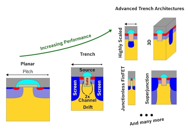
Figure 1. Advancement of SiC MOSFET device architectures over time. Image used courtesy of Bodo’s Power Systems [PDF]
Today, advancements in device design and manufacturing have closed the robustness gap, allowing SiC trench architectures to offer superior performance while matching the robustness and yield of their planar counterparts. Consequently, SiC trench gate power MOSFETs are now an excellent fit for all high-voltage systems in electric vehicles.
Advantages of SiC Trench Gate MOSFETs
With the upcoming transition to more advanced architectures, SiC trench gate MOSFETs are set to soon surpass planar architectures in both performance and robustness. Their smaller cell pitch, which results in lower conduction and switching losses, will make trench gate architectures a more desirable choice.
Bosch is one of the only manufacturers of SiC trench gate MOSFETs to date, combining high performance with solid robustness.
The evolution of SiC power device architectures over time (see Figure 1) illustrates the transition from conventional planar to trench and subsequently to advanced trench architectures. Bosch’s selfdeveloped dual-channel trench design allows for two electron channels in each unit cell, effectively halving the contribution of channel resistance to total on-resistance compared to single channel architectures.
Since channel resistance is one of the most important resistance contributions in the voltage classes typically used in electric vehicles (750 V and 1,200 V), the full utilization of the channel area yields a significant advantage.
In the future, advanced trench architectures can further reduce this key resistance contribution by lowering pitch size and increasing channel density. Additionally, these designs target JFET and drift zone resistance. Key trends include ultra-narrow pitch designs, the development of 3D structures by extending p-type contact regions and shielding regions into the third dimension, junctionless FinFET architectures, and trench superjunction devices.
Today’s trench designs should therefore be viewed as a starting point for the development of new MOSFET designs, which will ultimately achieve the lowest possible conduction losses and enhance the robustness of SiC power devices.
Reliability in Dual-Channel SiC Trench MOSFETs: Adding More Design Freedom
Key aspects of improving reliability in SiC trench gate architectures for automotive applications include the gate oxide quality as well as its robustness against cosmic rays. Figure 2 (top) shows the simulated electric field during off-state operation of a Gen2 Bosch dualchannel trench MOSFET. Bosch’s Gen1 to Gen3 utilize deep p-type ion implantation to push the electric field deep into the semiconductor.
This additional degree of design freedom is not present in planar SiC MOSFETs. Adapting the implant profile (doping, energy, implant angle) makes it possible to tailor the deep p-type screening and the current spreading regions, which constitute the JFET area. The electric field can thus be shaped to diminish electric field peaks, reducing both the electric field in the gate oxide and the field in the SiC itself.
A primary factor in ensuring the gate oxide’s long-term reliability is proper shielding against the reverse bias field, which is a main source of hole injection. The gate oxide of a SiC MOSFET is inherently more vulnerable than that of silicon-based counterparts. The higher defectivity at the SiC/SiO2 interface and the resulting larger number of extrinsic defects makes a significant gap between application and screening voltage essential.
This gap can be increased significantly with a thicker gate oxide. Since the cell pitch of trench gate MOSFETs is much smaller (and power density therefore higher), a thicker gate oxide can be implemented by sacrificing a small fraction of the on-state performance improvement. This increased gate oxide thickness enhances screening efficiency.
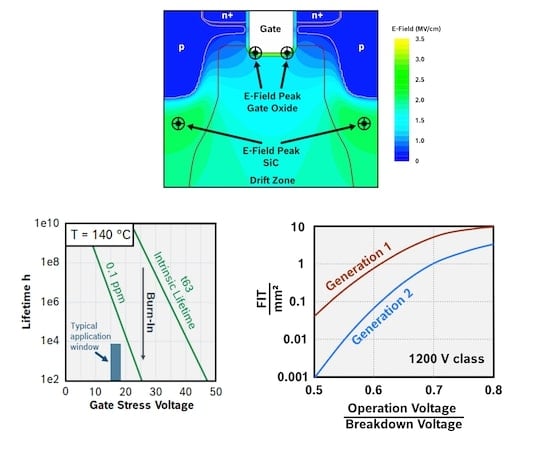
Figure 2. Top: Simulated electric field in a dual-channel trench gate MOSFET during the off-state. Left: Intrinsic lifetime of the gate oxide in Bosch’s SiC trench MOSFETs. Right: FIT rate dependency on blocking voltage for Gen1 and Gen2 SiC MOSFETs from Bosch. Image used courtesy of Bodo’s Power Systems [PDF]
Figure 2 (left) presents the intrinsic lifetime (t63) of the gate oxide in one of Bosch’s SiC trench gate MOSFETs, and the 0.1 ppm lifetime curve achievable through screening. Both the high intrinsic lifetime and the 0.1 ppm curve—which is well above the typical operating regime—demonstrate the excellent robustness of the gate oxide in this trench architecture.
The benefits of sophisticated shielding structures will be further enhanced with the introduction of advanced trench architectures. Since more compact designs enable more effective shielding, the gate oxide can be made even more robust, and gate oxide reliability in trenched devices is soon expected to surpass that of planar SiC MOSFETs.
While the intrinsic robustness of SiC trench gate MOSFET devices can achieve very high levels, factors such as cosmic ray impact cannot be overlooked. SiC devices are inherently susceptible to single-event burnout due to the high electric fields present during the off-state. Since cosmic ray impact cannot be avoided entirely, it must be mitigated to a level low enough to ensure low FIT rates.
Therefore, both the electric field shape and the definition of the breakdown voltage must be optimized. Here again, trench architectures present an important advantage: the JFET area below the trench can be tailored to reduce electric field peaks during blocking mode, leading to enhanced robustness against cosmic rays with little RonA penalty.
Figure 2 (right) illustrates the FIT rates for Bosch’s Gen1 and Gen2 1,200 V SiC trench gate MOSFETs with respect to the applied voltage.
By improving the electric field shape and increasing the breakdown voltage by 60 V, a 40x improvement in the FIT rate was achieved for operation at 50% of the breakdown voltage. The high cosmic ray robustness additionally makes it possible to utilize overvoltage transients (above the rated device voltage) for faster switching and lower switching losses.
Designing Future Generations
While transitioning from planar to trench and advanced trench gate MOSFETs is the best solution for applications with high power levels, the impact of these new designs on parallel operation in power modules needs to be carefully considered. In general, it is essential to avoid parasitic turn-on of a device in a power module while acting as a commutation partner.
A high Miller ratio (CGS / CGD) is therefore generally favorable, which can be easily achieved in trench gate and advanced trench gate SiC designs as narrower pitches and more compact designs will typically push CGD further down.
The example in Figure 3 shows the active turn-on/turn-off as well as passive turn-off of a future generation Bosch SiC MOSFET power module design study. Switching 1,000 A at 920 V in a module with four 40 mm² dies as physical switches demonstrates the complete omission of parasitic turn-on.
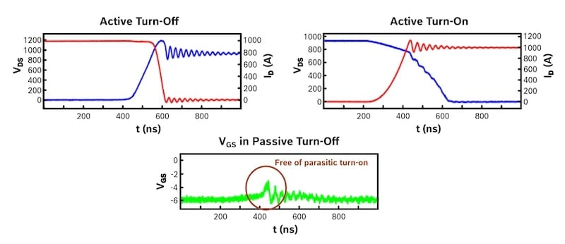
Figure 3. Switching characteristics of engineering samples of Bosch’s Gen3 SiC MOSFETs in a power module setup (920 V, 1,000 A). Image used courtesy of Bodo’s Power Systems [PDF]
However, reducing CGD can lead to unwanted self-excited oscillations in power modules, if they lack sufficiently low parasitic inductances in between parallel dies and exhibit a certain asymmetry for static and dynamic current sharing. In such modules, the power devices form an LCR circuit with the module inductances, leading to self-excited oscillations with the power MOSFETs acting as amplifiers. Damping these oscillations is possible by increasing the internal gate resistance per die.
However, this has negative consequences on system level, e.g. increased switching losses. Therefore, SiC MOSFETs should be designed to prevent these oscillations in the first place. This can be achieved by reducing the CDS/CGD ratio. However, this leads to a design trade-off, as a higher CGD is needed to dampen the oscillations, while a lower CGD is beneficial to avoid parasitic turn-on.
The full power density benefit of novel SiC trench gate MOSFETs can be exploited with modern power module architectures based on advanced assembly and interconnection technology (AIT). Figure 4 (top) shows the switching of a SiC MOSFET with a CGS/CGD ratio of 25 and a low RG,int of 2 Ω in a standard bond wire module.
In this conventional module, self-excited oscillations are clearly visible in the gate-source voltage, drain-source voltage, and drain current. Any further increase in the DC-link voltage or switched current can lead to catastrophic failure, even though the SiC MOSFETs are still far below their nominal current and voltage handling capabilities.
When switching to an advanced AIT module such as the Bosch Gen6 power module (Figure 4 right), these oscillations can be completely mitigated. Switching is consequently possible at much higher currents and DC-link voltages without any self-excited oscillations (Figure 4, bottom).
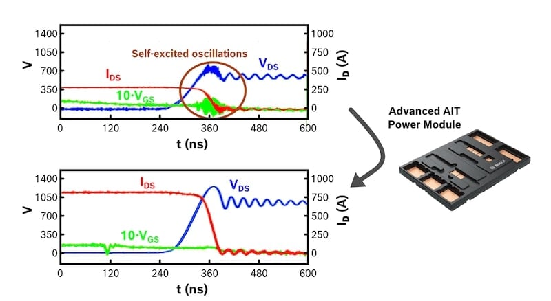
Figure 4. Turn-off switching characteristics for a standard bond-wire module and an advanced AIT power module. SiC power transistors with high CDS / CGD ratios were used to provoke self-excited oscillations in case of the standard bond-wire module. Image used courtesy of Bodo’s Power Systems [PDF]
Conclusion
SiC trench gate MOSFETs offer substantial benefits for both automotive and non-automotive applications, combining superior static and dynamic performance with high robustness unlike any other SiC power device technology. While today’s trench architectures already present a benchmark in terms of achievable power density, advanced trench-gate-based SiC architectures will further enhance this figure of merit, making trench gate MOSFETs the best choice among SiC devices.
This article originally appeared in Bodo’s Power Systems [PDF] magazine and is co-authored by Jens Baringhaus, Steffen Beushausen, and Klaus Heyers, all Robert Bosch GmbH