Facebook
 Google
 GitHub
 Linkedin
The Genesis of GeneSiC and the Future of Silicon Carbide
This article will examine GeneSiC MOSFETs and Schottky MPS diodes stretching from 650 V to 6.5 kV.
This article is published by EE Power as part of an exclusive digital content partnership with Bodo’s Power Systems.
Pioneers of SiC technology lead system efficiency with a paramount focus on reliability and ruggedness. For almost 20 years, GeneSiC has pioneered high-performance, robust, and reliable silicon carbide (SiC) power devices for automotive, industrial, and defense applications. As one of the first SiC device companies, GeneSiC developed cutting-edge SiC technologies for government bodiesⁱ, focused heavily on performance and robustness, and released several generations of both SiC diode and MOSFET technologies with ratings up to 6.5 kV in various packages as well as bare die.
In 2022, Navitas Semiconductor acquired GeneSiC Semiconductor, creating the industry’s only pure-play, next-generation power semiconductor company focused wholly on SiC and GaN. Dr. Ranbir Singh, who founded GeneSiC in 2004 and is now Navitas’ Executive Vice-President of SiC, has a rich history in SiC power technology, beginning with his research into the first SiC power devices at North Carolina University (NCSU). In 2022, to mark this pioneering work, Dr. Singh was inducted into the NCSU Electrical and Computer Engineering (ECE) Alumni Hall of Fame.

Figure 1. Residential homes can be powered by solar energy, BESS, an electric vehicle, and the grid. Image used courtesy of Bodo’s Power Systems [PDF]
With the industry’s broadest voltage range – stretching from 650 V to 6.5 kV – GeneSiC MOSFETs and Schottky MPS diodes have been at the forefront of SiC technology. The company has been involved with over 60 government-agency projects, pushing the boundaries of SiC performance, ruggedness, and reliability. These include the development of 6.5 kV SiC thyristors for energy storage, grid-tied inverters for the U.S. Department of Energy (DOE); 15 kV MOSFET and PiN diodes for defense applications; 500°C monolithically-integrated SiC super-junction transistor JBS diode (MIDSJT) for NASA’s Venus exploration missions, and monolithically-integrated, radiation-hardened SiC gate drivers for 1200 V SiC DMOSFETs and 6.5 kV SiC thyristors, for the U.S. Navy.
The SiC Market
The silicon carbide (SiC) market has expanded rapidly in the last few years thanks to a growing acceptance of the technology among engineers and an increased understanding of how to maximize the benefits of using wide bandgap power devices. Yole Développement forecasts that the SiC device market will grow beyond $6 billion by 2027, from only $1 billion in 202ii. A significant proportion of this growth will come from solutions for the automotive sector, solar energy storage systems, and industrial applications.
In 2022, electric vehicle sales in the United States surpassed 5% of the total passenger vehicle marketiii, joining 18 other countries that have achieved this threshold for mass adoption. However, there are still two main concerns for consumers wanting to transition to electric – range anxiety and charge times. Gasoline and diesel cars take less than five minutes to fill up, whereas with first-generation charging, EVs take at least 25 mins to charge up to 80%.
To address this issue, EV manufacturers are transitioning from 400 V to 800 V batteries, matched with roadside superchargers, with peak charging powers of 350 kW. Now, EVs such as the Genesis GV70 SUV using a Level 3, 800 V 350 kW DC charger can power from 10–80% in only 18 minutes. As well as higher power delivery, the increase in voltage also reduces I2R transmission power losses, lowering heat dissipation and reducing both cable weight and cost. To address the higher voltages, increased insulation is required in both the cables and motor windings, and the inverter system must be designed to match. Thanks to their increased efficiency and performance improvements at higher voltages, 1,200 V SiC MOSFETs are ideally suited to addressing this requirement.
Using an EV to Power Your House
The average battery size in an electric vehicle is 40 kWhriv. Being four times the size of an average residential battery energy storage system (BESS)v, this means an EV can quite easily deliver the energy needed by a typical house for the whole day. Offering this alternative ‘vehicle-to-home’ (V2H) approach will become a disruptive driver in the industry and change the way we use energy in the future. Accessing power from the EV will save electricity costs and reduce strained demand on the grid, while re-charging the EV when demand and costs are low drives down household bills and support better grid stability. What’s more, the EV can also provide energy back to the grid (V2G) when the demand is high. This has the potential to transform the utility grid to make it more intelligent and dynamic, with electricity transferred and stored at a macro scale.
With this in mind, EV manufacturers are now starting to introduce bi-directional onboard chargers (OBCs), which provide a two-way street of power delivery for V2H, V2G, and vehicle-to-load (V2L). The Nissan Leaf, Ford F-150 Lightning, Hyundai Ioniq 5, Kia EV6, and the Mitsubishi Outlander PHEV all offer this capability today.
Such next-generation integrated and holistic power solutions are increasingly reliant on SiC power devices. SiC MOSFETs such as those in the GeneSiC family, for example, can provide the high temperature, high-speed performance that these applications demand, while GeneSiC merged-PIN Schottky (MPS) SiC diodes must sustain excessive surge currents with low leakage while offering low forward-voltage drop and fast-switching characteristics.
Fast Charging Stations
The GeneSiC's history to address the needs of the automotive sector also includes the development of solutions for the fast-charging stations that are essential to the rapid adoption of EVs. Take, for example, SK Signet’s recent design for a 350 kW-rated fast charger that converts 277 VAC mains electricity to a carefully-controlled 200- 950 VDC for both 400 and 800 V-rated battery-powered electric vehicles. Each fast charger uses 168 x 1,700 V-rated GeneSiC diodes in the input power-factor correction (PFC) and output-rectifier stages to provide efficient, robust operation. The high-performance GeneSiC components operate up to 12 °C cooler than competing devices due to extremely-low threshold voltage (VTH) characteristics, which maximizes energy savings and supports longer lifetime operation.
Fast charging is also a key requirement in the industrial sector, where, again, GeneSiC technologies are being deployed to address application-specific challenges. Exide Technologiesvi, for example, has adopted new, leading-edge GeneSiC power semiconductors to ensure reliability, safety, ease of use, and optimal charging in its next generation of high-frequency fast chargers for industrial materials-handling equipment.
Exide’s 2100-series fast chargers convert 220 V AC power to a battery-level voltage between 24 and 80 V for automated guided vehicles (AGVs) and manned material handling equipment such as forklifts and pallet trucks. Each 7 kW module uses GeneSiC 750 V MOSFETs and MPS Schottky diodes with frequency-optimized architecture. The same platform can be upgraded to 10 kW, with four modules in parallel to provide 40 kW of reliable fast-charging power.
Solar Energy
Another significant growth driver for SiC is energy management in areas such as solar conversion, wind energy, heat pumps, and energy storage.
In recent years, we have seen an increased number of power outages due to weather conditions and climate change. In 2021, there were 350 million outages worldwide, and in the United States, approximately 83% of reported major outages were attributed to weather-related eventsv. With the stability of the grid in question, customers are resorting to installing solar power and BESS technologies in their homes and businesses. Indeed, the U.S. ‘attach rate’ for battery storage capability sold with solar panels has increased from 9.5% to 17.1% in only 18 months. Having energy independence and being able to live off-grid not only provides security but also allows customers to optimize and manage energy storage and usage for lower electricity bills – an increasingly important issue in a market where utility costs keep increasing.

Figure 2. GeneSiC trench-assisted planar-gate technology enables leading-edge performance with high-yielding manufacturing. Image used courtesy of Bodo’s Power Systems [PDF]
GeneSiC has been established in the solar market for several years, and its technologies can be found in a variety of inverters, including KATEK’s Steca coolcept fleX seriesvii, which convert DC power from a string of solar panels into 4.6 kW AC power for use in the home, returning to the grid, or being stored locally for later use.
Each inverter uses sixteen GeneSiC 1200 V, 75 mΩ-rated SiC MOSFETs to provide a two-level converter with bi-directional boost converters and an H4-topology for AC voltage output. As well as delivering the performance and reliability needed by this application, the increased switching frequency of the SiC technology allows the size and weight of passive components to be reduced, which optimizes the KATEK unit in size and weight compared with legacy silicon-based inverters.
Energy Storage
The average U.S. home uses 29 kWh per dayviii, a demand that typically requires 20-25 solar panels. Assuming the roof receives four hours of sunlight each day and each panel provides 350 W of power, then 22 panels would be required. The problem is that approximately 30% of electrical usage happens during solar production hours. Midday has the strongest daylight and provides the most power, yet the majority of homeowners are at work and not able to use this free energy.
Storing this energy from the sun for later use means that when a homeowner arrives home in the evening - which is when electricity costs from the grid are at a peak - they can switch over to the battery system. This reduces utility bills and optimizes how the energy is distributed.
There are several ways to store energy in the BESS, including solar energy, grid connection, and, as mentioned previously, energy from an EV.
A BESS consists of a battery module, a battery management system (BMS), an energy management system (EMS), and a power conversion system (PCS). Typical systems range between 10-20 kW, which translates to powering a home for anything between eight and 16 hours. Wide bandgap devices, such as SiC MOSFETs and GaN power ICs, are used in the inverter and buck-boost stages of these systems to convert AC-DC (from grid to battery), DC-DC (from solar to battery) and DC-AC (from battery to grid or battery to home).
SiC Technology Update – MOSFETs
The imperative to deliver ever-higher performance and more efficient energy conversion and control while supporting environmental sustainability through the electrification of our world and the reduction of CO2 emissions is driving the ongoing development of SiC solutions for mass market applications. Take, for example, GeneSiC trench-assisted planar gate MOSFET technology.
While SiC MOSFETs offer superior conductivity and switching performance compared to silicon due to their wide bandgap characteristics and high electric-field strength, traditional designs using planar or trench techniques have had to compromise between manufacturability, performance, and/or reliability. The patented GeneSiC trench-assisted planar-gate design, however, is a no-compromise, next-generation solution that supports high-yield manufacturing, fast and cool operation, and extended long-life reliability. Combined with the industry’s lowest RDS(ON) at high temperatures and lowest energy losses at high speeds, these devices enable unprecedented, industry-leading levels of performance, robustness, and quality.
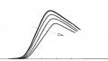
The issue of RDS(ON) and temperature is particularly important. In real-life applications, the ambient temperature in a system can be up to 80 °C, with device power cycling further elevating junction temperature. GeneSiC MOSFETs were designed with this in mind and support the industry’s lowest RDS(ON) temperature co-efficient. In datasheets, RDS(ON) is typically rated at 25 °C, but depending on the temperature coefficient, this can significantly increase at elevated temperatures. In tests, a GeneSiC 1200 V, 40 mΩ SiC MOSFET in a D2PAK was compared against the comparable leading SiC MOSFET technology, and the equivalent gate drive and conditions were realized to reveal a true comparison. The results demonstrated that GeneSiC MOSFETs operate with a 25 °C cooler case temperature, which results in significantly lower losses and higher system efficiency. From a reliability standpoint, 25 °C cooler operation translates into a three times longer device lifetime.
Other important ‘figures of merit’ for evaluating SiC MOSFETs are resistance and area and resistance and gate charge.
The latest Yole SystemPlus SiC Transistor 2022 Report compared twelve SiC MOSFET technologies for RDS(ON)*Area and RDS(ON)*QG, and the results show that GeneSiC’s novel MOSFET technology outperforms all competition, including trench gate structures, whilst keeping the benefits or planar gate ruggedness, short circuit capability and simpler manufacturing processing.

Figure 3. Operating temperature comparison. Image used courtesy of Bodo’s Power Systems [PDF]

Figure 4. GeneSiC’s pioneering MOSFET technology leads the industry and is proven by third-party evaluation. Image used courtesy of Bodo’s Power Systems [PDF]
In 2019, GeneSiC collaborated with Sandia National Laboratories and DoE to create a state-of-the-art, leading-edge monolithically integrated SiC double-implanted metal oxide semiconductor (DMOSFET) device structure with a merged PiN Schottky (MPS) diode. This product was later awarded Green Tech special recognition at the 100 R&D Awards. Integrating a JBS diode within the MOSFET provides more efficient bi-directional performance, temperature-independent switching, low switching and conduction losses, reduced cooling requirements, and superior long-term reliability. Typical applications are ‘medium-voltage’ power conversion systems, such as traction, pulsed power, and smart grid infrastructure.
Monolithic integration of the MOSFET and diode enables low conduction losses during the operation of the free-wheeling diode without an externally connected Schottky diode. Furthermore, the built-in P-Well/N-Drift body diode of the MOSFET structure is bypassed, which can lead to faulting of the basal plane dislocations (BPDs) present within the N- drift layer of the MOSFET.

Figure 5. GeneSiC MOSFET with monolithically-integrated MPS diode increases efficiency in 3rd quadrant operation and significantly improves reliability. Image used courtesy of Bodo’s Power Systems [PDF]

Figure 6. 3.3 kV Monolithic MOSFET with MPS diode has a significantly lower voltage drop in the third quadrant operation compared to a discrete SiC MOSFET. Image used courtesy of Bodo’s Power Systems [PDF]

Figure 7. Using 3.3kV SiC MOSFETs with integrated Diode reduces the number of devices in series and improves system efficiency and reliability while reducing weight, size, and cooling requirements. Image used courtesy of Bodo’s Power Systems [PDF]
The benefits that this technology offers can be seen by considering the implementation of a medium voltage (MV) grid-to-battery energy storage system in which the MV grid is connected to the BESS by an isolated topology, such as a dual active bridge (DAB) and an active front-end converter (AFEC). A three-level, neutral-point clamped (NPC) inverter reduces filter requirements compared to a two-level topology, lowering the voltage stress across the SiC MOSFETs.
A series connection of the SiC 3.3 kV MOSFET-diode devices is possible, depending on the grid voltage (Figure 7), while the low-voltage side is supported by 1200 V SiC devices. The medium frequency transformer switching frequency can range from 10 - 20 kHz. Single or a three-phase topology can be used depending on the power requirements. Using single 3.3 kV SiC MOSFET-diodes as a replacement to several 1.2 - 1.7 kV MOSFETs or IGBTs connected in series has significant advantages, including easier gate driving, lower parasitic inductance, reduced conduction losses, and higher system efficiency. Cooling requirements can be substantially reduced, alongside system size and weight.
SiC Technology Update – Diodes and Modules
At PCIM 2023, Navitas announced the 5th generation of merged-PIN Schottky (MPS) diodes with low-built-in voltage biasing technology, offering superior FOM and the highest robustness to provide industry-leading efficiencies in SMPS PFC applications across all load situations. The novel design of the MPS diode combines the best features from both PiN and Schottky diode structures, producing the lowest forward voltage drop (VF), high surge-current capability (IFSM), and minimized temperature-independent switching losses. Proprietary thin-chip technology further reduces VF and improves thermal dissipation for cooler operation.
Additionally, the Gen 5 MPS diodes have been designed for best-in-class robustness and ruggedness for applications demanding high surge current and avalanche capability, critical for fail-safe designs. All GeneSiC devices are 100% avalanche (UIL) production tested to ensure the highest level of ruggedness in over-voltage conditions.
These devices are ideal in PFC circuits in continuous current mode (CCM) due to excellent figures of merit, comprising a low VF of 1.3 V and minimized capacitive charge (QC). In addition, zero reverse recovery charge improves PFC MOSFET turn-on performance. The result is a cooler, more reliable system.

Figure 8. GeneSiC Gen 5 650V diodes have a novel structure enabling low-built-in voltage biasing while providing an excellent figure of merit (QC.VF). Image used courtesy of Bodo’s Power Systems [PDF]

Figure 9. In a 3 kW Interleaved Boost PFC, GeneSiC diodes offer the highest system efficiency across light and full load due to superior FOM. Image used courtesy of Bodo’s Power Systems [PDF]
SiCPAK SiC MOSFET Modules
Navitas has also announced the availability of its module packaging portfolio, starting with the SiCPak moduleix. These industry-standard press-fit modules have been designed with performance, reliability, and ruggedness at the forefront. The G3 1200V MOSFETs range from 6mOhms upwards in half-bridge configurations. The SiC MOSFETs are Ag sintered to provide superior thermal dissipation and reliability. Additionally, the Direct-Bonded Copper (DBC) substrates are manufactured by Active Metal Brazing (AMB) on silicon nitride (Si3N4) ceramics ideal for high-power cycling applications. The excellent bending strength, high fracture toughness, and excellent thermal conductivity make silicon nitride (Si3N4) well-suited for power electronic substrates.
Growth markets such as electric vehicles, renewable energies, and energy storage are driving higher system efficiency requirements that only SiC power devices can enable. To learn more about the high-performance GeneSiC range, and how dedicated Navitas Design Centers can provide complete platform designs to upgrade and accelerate your design, visit navitassemi.com.
References
i SBIR.gov (2023) ‘GeneSiC Semiconductor’ https://www.sbir.gov/sbc/genesic-semiconductor-inc?page=4
ii Yole Developpement (2022) ‘Power SiC 2022’. https://s3.i-micronews.com/uploads/2022/03/Power-SiC2022-Product_Brochure.pdf
iii Statzon (2023) ‘US EV Market Share Has Surpassed the 5% Tipping Point’ https://statzon.com/insights/us-ev-market https://statzon.com/insights/us-ev-market
iv E.ON Energy (2023). ‘Electric car battery capacity & lifespan’ https://www.eonenergy.com/electric-vehicle-charging/ costs-and-benefits/battery-capacity-and-lifespan. html#:~:text=Electric%20car%20battery%20capacity,- Lithium%2Dion%20battery&text=The%20average%20capacity%20is%20around,higher%20the%20kWh%20the%20better.
v Solar.com (2023)/ ‘How Long Can Solar Battery Power a House During an Outage?’ https://www.solar.com/learn/how-long-can-a-battery-providepower-during-an-outage/#:~:text=Home%20battery%20 capacity&text=Battery%20storage%20capacity%20is%20 measured,is%20typical%20for%20most%20homes.
vi Navitas (2023) ‘Navitas’ Next-gen SiC Power Semis Adopted in Industrial Chargers from Exide Technologies’ https://navitassemi.com/navitas-next-gen-sic-power-semisadopted-in-industrial-chargers-from-exide-technologies/
vii Navitas (2023) ‘Navitas and KATEK Accelerate Solar Adoption with Higher Efficiency and Lower Costs’ https://navitassemi.com/navitas-and-katek-accelerate-solaradoption-with-higher-efficiency-and-lower-costs/
viii EIA (2022). ‘How much electricity does an American home use?’ https://www.eia.gov/tools/faqs/faq.php?id=97&t=3 ix Navitas (2023). ‘Navitas Launches into High-Power Markets with GeneSiC SiCPAK™ Modules and Accelerates Bare-Die Sales’ https://navitassemi.com/navitas-launches-into-high-powermarkets-with-genesic-sicpak-modules-and-accelerates-bare-diesales/
This article originally appeared in Bodo’s Power Systems [PDF] magazine.
Related Content