Facebook
 Google
 GitHub
 Linkedin
An Enhanced TO-247 Package Significantly Lowers SiC MOSFET Temperature
ISOMOS from Analog Power Conversion, LLC, (APC-E)/Luminus [1] improves on the thermal performance of the popular TO-247 package used in many SiC-based designs, enhancing reliability and simplifying assembly without resorting to expensive modules.
Article co–authored by Martin Held, Senior Engineer at Analog Power Conversion, (APC-E) / Luminus.
This article is published by EEPower as part of an exclusive digital content partnership with Bodo’s Power Systems.
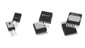
The ubiquitous TO-247 package remains a cornerstone in power electronics for high-reliability applications due to its superior high-voltage power-handling ability relative to other discrete packages. Despite the growing share of SMT and Top-side cooled packages, it retains a dominant market share [2] for discrete power devices, and it will continue to grow along with the growth in applications such as traction inverters, chargers, energy storage, solar/wind inverters, datacenter power supplies, and industrial motor drives.
Standard TO-247 variants require external electrical isolation materials for safe heatsink mounting. These isolating materials introduce significant thermal penalties. This report evaluates the thermal performance of an advanced TO-247 package with an internal Direct Bonded Copper (DBC)[3] ceramic isolating element, specifically, an Aluminum Nitride (AlN) substrate providing 2.5 kV isolation, against the standard non-isolated TO-247 with external thermal/ electrical isolation interface materials.
Thermal modeling and experimental measurements demonstrate a reduction of junction-to-sink thermal resistance of approximately 60% compared with standard TO-247 devices using isolation pads. This improvement results in a 41% lower junction temperature and enables significant system-level benefits, including increased power density, reduced heatsink requirements, and simplified assembly.
ISOMOS – TO-247 with High Performance Integrated Ceramic DBC Element
The motivation to employ wide bandgap devices like SiC MOSFETs is to achieve greater power efficiency and increase power density for more compact systems. Conventional TO-247 packages pose challenges in this regard with sub-optimal thermal performance. The standard TO-247 package has an electrically conductive tab typically at the MOSFET Drain potential for mounting to a coldplate/heatsink. For purposes of electrical safety, i.e., reduced shock hazards, and improved noise margin, it is desirable to electrically isolate the mounting tab from the heatsink, especially in cases where multiple devices operate at different potentials.
his is typically accomplished using thermally conductive but electrically isolating ceramic, mica or similar Thermal Interface Materials (TIM). These elements often complicate assembly and increase thermal resistance from the package to the heatsink, impacting thermal performance. Alternatively, the ISOMOS package from APC Electronics (APC-E) [1] moves the thermal-electrical isolation layer inside the package. The DBC utilizes a highly thermally conductive ceramic, Aluminum Nitride (AIN), with copper bonded to both sides of the ceramic substrate via a high-temperature oxidation process. This creates a much shorter and more efficient thermal path from the silicon die to the heatsink compared to external thermal interface materials (TIMs) for isolation.
AIN has amongst the highest thermal conductivity, approximately 200W/m-k, of ceramic insulating materials. Its thermal conductivity is ~6x higher than Alumina and ~2.5x higher than Silicon Nitride, which are also popular ceramic materials used for isolation. Additionally, ISOMOS offers a guaranteed and tested 2.5kV RMS isolation voltage compliant to UL 1557[4]. While the ISOMOS and the standard TO-247 share identical external dimensions, their internal construction is quite different.
Referring to Figure 1, the standard TO-247 requires external electrical isolating foil, whereas the ISOMOS requires nothing more than the application of a thin layer of thermal grease to fill in any microscopic voids between the heatsink and backside tab. The elimination of external isolation pads simplifies assembly and enables more consistent automated manufacturing as an engineered solution rather than a manually assembled one. As opposed to ISOMOS, the standard TO-247 requires manual application of foil and related materials, introducing errors caused by misalignment and/or uneven pressure of the isolated pads.
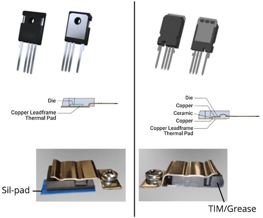
Figure 1. Comparison between the standard TO-247 and ISOMOS™ with integrated DBC. Image used courtesy of Bodo’s Power Systems [PDF]
The Performance and Quality Advantage of ISOMOS
In summary, we find the following benefits offered by ISOMOS:
Lower Thermal Impedance ➞ Better Thermal Performance
- Internal DBC provides a solid, highly conductive copper-ceramic path from die/package base to heatsink, allowing SiC MOSFETs to run cooler. Also note that thermal isolation pads/foil vary widely in terms of performance and long-term stability.
Improved Reliability and Long-Term Stability
- Reduced thermal stress can increase device lifetime or allow higher current/power per device. Lower die temperatures (e.g., 20–30°C cooler in DBC vs. TIM) means enhanced reliability; A commonly used reliability rule of thumb is that failure rate halves for each 10°C reduction in junction temperature (Arrhenius acceleration model).
- Excellent Coefficient of Thermal Expansion (CTE) matching. – The Aluminum Nitride (AlN) ceramic in the isolated ISOMOS package is engineered for minimal Coefficient of Thermal Expansion (CTE) mismatch with the Silicon Carbide (SiC) die.
Simplified Assembly & Lower Recurring Labor Over Time
- No need to cut/align pads, apply grease, inspect pad placement/ flatness - simpler assembly flow. Saves labor per device once implemented and associated costs. Reduced assembly steps reduce chances of human error (misalignment, improper torque, grease smear/uniformity issues), which improves yield and reduces rework.
System-Level Benefits
- Because of better thermal efficiency, the number of devices can be reduced (higher current per device). Additionally, the heatsink size, cooling system, or derating margin shrinks - reducing overall system cost/size/complexity, resulting in Improved power density.
- Reduced parasitic drain-to-heatsink capacitance due to common heatsink improves switching performance and reduces EMI • For rugged applications (automotive, industrial), improved thermal and isolation reliability adds to product lifetime - important for warranty, maintenance, brand reputation.
- Overall efficiency of the system will be improved based on the simple fact that the ON Resistance of the SiC MOSFET will be lower at lower junction temperatures.
Cost Advantages at Scale
- Even with a modest package adder, for multidevice systems, the integrated DBC approach becomes cheaper than pad + grease + labor once you include recurring assembly costs and pad/grease materials. Many systems employ over 48 MOSFETs, which further increases system complexity and cost.
System Thermal Performance Comparison – ISOMOS™ vs Standard TO-247
To demonstrate the thermal advantage of ISOMOS, a comparison between ISOMOS and a standard non-isolated TO-247, along with a popular TIM, was made. A material with thermal conductivity equal to 1.8W/m-k was selected as the TIM used with the non-isolated 1200V, 13mW, TO-247 package and compared to one of the similar-rated devices in the ISOMOS family. Please refer to Table 1, where measured and calculated thermal impedances were compared.
For reference, let us recall the basic thermal Ohm's law per Figure 2.
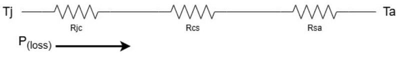
Figure 2. Basic Thermal Stack. Image used courtesy of Bodo’s Power Systems [PDF]
Thermal Ohms Law: Tj -Ta = P(loss) * (Rjc + Rcs + Rsa) where,
Tj = Junction temperature. Source of heat.
Ta = Ambient Temperature
P(loss) = MOSFET Power loss
Rjc = Junction-Case thermal Resistance of the TO-247 package
Rcs = Typically some form of TIM and/or Grease
Rsa = Sink-Ambient thermal resistance of heat sink
Tj -Ta represents the total thermal budget for a system. Thermal resistances add up, reducing the available budget, which designers work to minimize. The thermal resistance of ISOMOS, being significantly less than standard TO-247 using external isolation materials, provides more headroom for increased power density or keeping the same power density but at lower system cost and lower junction temperature of the SiC switch.
We will use a standard method used to compare the thermal impedance, Rθ(pad), of Thermal Interface Materials (TIMs) such as the sil pad used here.
Rθ(pad) = Zθ/A, where Zθ is the thermal impedance specification and A = thermal pad contact area of a TO-247 package.
For the sil pad, from the datasheet, Zθ = 0.28 (°C-in2/W) @ 25psi.
For the TO-247, we assume the contact area A=0.33in2.
Rθ(pad) = Zθ/A = 0.28 (°C-in2/W)/0.33in2 = 0.85°C/W.
We add the junction-case thermal resistance from Figure 3 package to Rθ(pad) for the total thermal stack, junction - sink, Rθ(js).
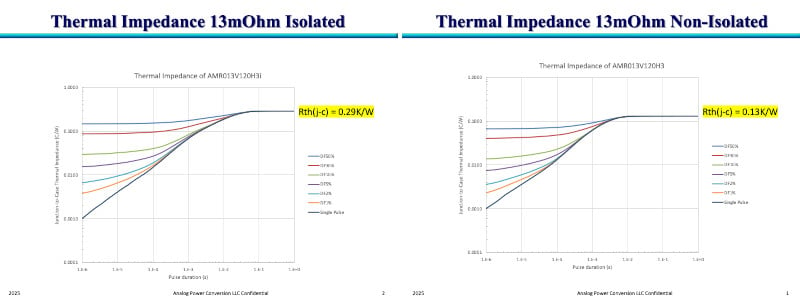
Figure 3. Thermal Impedance Curves for both Standard TO-247 AMR013V120H3 and ISOMOS AMR013V120H3i. Image used courtesy of Bodo’s Power Systems [PDF]
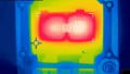
Rθ(js). = Rθ(jc) + Rθ(pad) = 0.13°C/W + 0.85°C/W = 0.98°C/W which correlates to the 1.06°C/W measured value. A heating current of 1.5A was applied at 50V drain voltage, increasing the MOSFET Pdiss to 75W. Thermocouples were placed on the heatsink and die junctions to accurately measure temperature, as shown in Figure 4.
Table 1. Thermal Impedance Comparison.
|
Device and Isolation Type |
Rth °[C/W] |
Measured Temperature |
|
TO-247 with 1.8W/m-K isolation pad |
1.06 measured VS 0.98 calculated |
111°C |
|
ISOMOS- - 1200V, 13mΩ, Isolated TO-247 package |
0.42, per Figure 3, measured incl grease (grease adds ~ 0.2) |
79°C |
The results as shown in Table 1 demonstrate the thermal advantage of ISOMOS. A significant 41% lower junction temperature using just a thin layer of Aavid Ther-o-Link thermal grease for proper mounting to the heatsink. At 111 °C, the maximum operating temperature is close to exceeding recommended operating conditions. Beyond this temperature, system reliability may be impaired. ISOMOS keeps the temperature at 79°C, well within normal operating conditions.

Figure 4. Thermal Measurement. Image used courtesy of Bodo’s Power Systems [PDF]
Additionally, the 46°C delta consumes less of the thermal budget as discussed previously and increases the thermal headroom that can be used in the design stage for increasing the output power for the same system without additional cost. Alternatively, consideration may be used to reduce system size, including the heatsink, sized for smaller power losses, or increasing switching frequency for smaller inductors and capacitors.
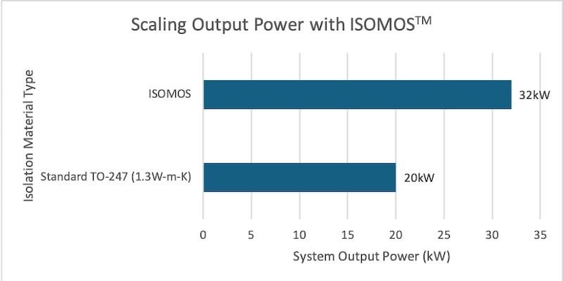
Figure 5. Estimated Output Power Comparison. Image used courtesy of Bodo’s Power Systems [PDF]
Increasing Output Power with ISOMOS
In scaling output power to 20kW, for example, the advantages of ISOMOS become more apparent. Using the measured values of thermal resistance, a model was created to estimate power losses. At a 20kW output level, there will be 300W power loss at 98.5% efficiency.
From our thermal Ohm's Law in Figure 2, we can estimate that using the same 1200V, 13mΩ MOSFETs but with the integrated ceramic DBC, the system output can increase to over 30kW, as shown in Figure 5 in the same enclosure. The extra thermal headroom in such a system may also be utilized to reduce the number of parallel MOSFETs per switch position and significantly reduce system cost and size.
Summary and Conclusions
Addressing the needs of increasing power levels offered by Wide Bandgap (WBG) semiconductors like SiC MOSFETs requires engineers to carefully consider advanced packaging to increase power density. ISOMOS from APC-E, with its integrated high thermal-conductivity Direct Bonded Copper (DBC) ceramic element, has been shown here to help designers address these issues without the necessity of moving toward expensive modules.
Compared to a standard non-isolated TO-247, ISOMOS has been shown to significantly reduce the junction-to-heatsink thermal resistance compared to that of a standard TO-247, resulting in a 32°C lower junction temperature at 75W. When scaling this advantage to higher power levels, such as 20kW, we see the DBC-integrated ISOMOS delivers ~60% more power in the same footprint.
Capitalizing on the extra thermal headroom, the designer can now choose higher Rds(on) MOSFETs at lower cost for a given output power or a reduction of heatsink size with lower losses and increasing power density.
Beyond upfront cost, the ISOMOS delivers measurable reliability and thermal advantages that reduce lifetime cost. The integrated ceramic DBC provides a stable, low impedance thermal path with excellent CTE matching to SiC die, avoiding silicon pad creep, grease pumpout, and torque-dependent thermal degradation over time.
This results in lower and more stable junction temperatures, improved thermal cycling robustness, and reduced maintenance or field failure risk. Essentially, ISOMOS from APC-E helps extend the legacy of the very popular high-power TO-247 package into the future.
References
[1] APC Electronics (APC-E) designs and develops advanced SiC products. Luminus, www.luminus.com/products/power-products, is the exclusive marketing and sales partner
[2] Yole Group, 2025 Reports
[3] Wikipedia - Power electronic substrate. Link: Power electronic substrate - Wikipedia https://en.wikipedia.org/wiki/Power_ electronic_substrate
[4] UL 1557 | Electrically Isolated Semiconductor Devices https://www.shopulstandards.com/ProductDetail.aspx?UniqueKey=43738
This article originally appeared in Bodo’s Power Systems [PDF] magazine and is co-authored by Lawrence Mazer, FAE Manager and Martin Held, Senior Engineer; Analog Power Conversion, (APC-E) / Luminus