Facebook
 Google
 GitHub
 Linkedin
SiC MOSFET Enhances Stability Under Real Application Conditions
The recently launched 1200 V CoolSiC™ MOSFET M1H comes with a variety of new features and improvements from which the targeted applications will benefit. One highlight is the much-improved stability of the threshold voltage under real application conditions.
Introduction
The drift of threshold voltage (VGS(th)) under real application conditions has been a SiC-specific focus in the last couple of years.
Infineon first discovered the drift phenomenon in VGS(th) under long-term stress caused by dynamic operations and presented recommendations for an operation gate voltage area to minimize drift over the lifetime. [1]. After ongoing research and subsequent optimization, the newly launched CoolSiC™ MOSFET M1H now shows a significant improvement in VGS(th) stability with a negligible impact of the drift effect in almost all cases.
Phenomenological Description
VGS(th) drifts are typically characterized by high-temperature gate bias stress tests (DC-HTGS) that follow the test guidelines defined in standards such as JEDEC. Recent findings indicate that bipolar AC gate stress including < 0 V can lead to a higher threshold voltage drift than corresponding static gate-stress tests would imply (DC-HTGS). This finding presents a new perspective in SiC MOSFET device reliability [1,3].
Figure 1 shows the different impacts of AC & DC stress conditions. The data of the change in VGS(th) (ΔVth) was derived using maximum conditions from the datasheet [1]. Two different slopes are visible, the first corresponding to a typical DC-like drift behavior (“DC fit”). The second larger slope is due to the bipolar AC stress effect (“AC fit”) also referred to as gate switching instability (GSI).
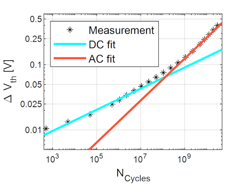
Figure 1. Drift during continuous gate switching stress: = 20 V; = −10 V; = 150 °C and = 500 kHz. [1]. Image used courtesy of Bodo’s Power Systems
We conclude that under stress conditions exceeding 108 switching cycles, the AC drift is the main contributor to stress, while the DC drift is the main cause of stress for fewer switching cycles.
The data shows that switching stress leads to a slow VGS(th) increase over time. Due to the increase of the threshold voltage VGS(th) an increased channel resistance (Rch) can be observed. This phenomenon is described in equation (1), where L is the length of the channel, W is the width of the channel, μn is the electron mobility, Cox is the gate oxide capacitance, VGS(on) is the on-state gate voltage, and VGS(th) is the threshold voltage of the device [1].
\[R_{ch}\approx\frac{L}{\mu_{n}\cdot C_{ox}\cdot W\cdot (V_{GS(on)}-V_{GS(th)})}\,\,\,\,\,\,\,(1)\]
The total RDS(on) is determined by the sum of the single resistances. These are channel resistance (Rch), the resistance of the junction field-effect transistor (RJFET), the epitaxial layer resistance of the drift region (Repi), and the resistance of the highly doped SiC substrate (RSub). The entire chain for the total RDS(on) is described in equation (2).
Thus, the increase of VGS(th) causes slight increases in the channel resistance, followed by the RDS(on), and in the on-state losses over time.
\[R_{DS(on)} = R_{ch}+R_{JFET}+R_{epi}+R_{Sub}\,\,\,\,\,\,\,(2)\]
Gate Switching Stress
To secure and predict long-term electrical parameter stability of our CoolSiCTM MOSFETs during typical switching operations, we have developed and applied a new qualification stress test: the gate switching stress test (GSS). This test enables you to directly determine electrical parameter drifts that typically run in bipolar mode (positive VGS(on) for turn-on and negative VGS(off) for turnoff) under application-like gate switching conditions. This test is a must for qualifying SiC MOSFETs, as it enables developers to quantify the new failure mechanism described above.
The GSS test covers all important drift phenomena, including those that occur during normal device operation. Except for the missing load current, which itself does not alter the observed drift behavior [3], we mimic the application as closely as possible by keeping gate switching characteristics, such as voltage slopes, similar to typical application conditions (see figure 2) [1]. To cover potential impacts of over-and undershoots in the gate signal, which is common in real SiC MOSFET applications, we apply worst-case conditions by stressing at the allowed maximum gate voltages from the datasheet and the maximum static junction temperatures (Tvj,op).
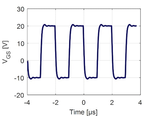
Figure 2. Typical GSS gate-source stress signal at a frequency of f=500 kHz [1]. Image used courtesy of Bodo’s Power Systems
The testing under worst-case conditions makes customers feel confident that they can use the device over the entire specification range without ever exceeding the drift limit. Hence, the approach guarantees excellent device reliability combined with easy calculation of safety margins. Besides VGS(th), other parameters like the gate leakage current are also measured and remain constant over time for the tested hardware [1].
Assessment of Worst-case end-of-life Drift and Impact on the Application
One of the main tasks during the development of an inverter is to predict the lifetime of the device. Therefore, it is necessary to have reliable models and information available. After extensive tests under various operating conditions, we were able to develop a predictive, semi-empirical model that describes the change in threshold voltage as a function of the relevant mission profile parameters such as stress time (tS), gate bias low level (VGS(off)), gate bias high level (VGS(on)), switching frequency (fsw) and operation temperature (T) (ΔVGS(th)(tS, VGS(off),VGS(on), fsw, T)) [3].
Based on the model, we have established a method of assessing the threshold-voltage drift with a worst-case end-of-application profile (EoAP) to calculate the relative drift. For applications that run at an arbitrary frequency for certain times, we calculate the total number of switching cycles (NCycle) until EoAP. NCycle can then be used to read out the relative drift.
The number of cycles depends on the switching frequency and the operating time. Typical hard-switching industrial applications, such as solar string inverters, make use of a switching frequency between 16 to 50 kHz. Inverters that use resonant topologies often switch faster than 100 kHz. The lifetime targets of these applications are typically between 10 to 20 years, while the real operating time is often between 50 percent to 100 percent.
The following example shows a sample evaluation:
- Targeted lifetime [years]: 20
- Real operation time [percent]: 50 => 10 years
- Real operation time [s]: 315360000 s (10 years)
- Switching frequency [kHz]: 48
- Cycle duration [s]: 1 / switching frequency = 0.0000208
- Number of cycles at end of life: operating time / cycle duration = ~1.52E+13
For a turn-on voltage of 18 V, a relative RDS(on) change of less than 6 percent at 25°C and less than 3 percent at 175°C can be expected, as shown in figure 3.
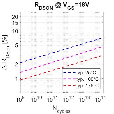
Figure 3. Relative RDS(on) change at VGS(on) = 18 V, Tvj,op= 25°C, 100°C & 175°C [2]. Image used courtesy of Bodo’s Power Systems
The example shown in figure 4, based on the recently launched EasyPACK™ FS55MR12W1M1H_B11 (six-pack configuration in a DC-AC inverter), illustrates the impact of the predicted change in RDS(on) [4]. The example shows applications in which conduction losses (Pcon) represent a big portion of the loss distribution. Tvj,op rises only by 2 K from an initial 148°C to the worst-case EoAP of 150 °C. The result confirms that a slight change in RDS(on) leads to a negligible increase in Tvj,op even after 20 years’ lifetime.
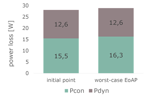
Figure 4. Worst-case EoL assessment: Vdc: 800 V, Irms: 18 A, fout: 50 Hz, fsw: 50kHz, cos(φ): 1, Th = 80 °C. Image used courtesy of Bodo’s Power Systems
This approach implies that the largest drifts should be expected under the worst-case conditions described. With the new M1H hardware, customers will be able to choose the parameter set from the data sheet’s specification range that best fits their application. Parasitic overshoots and undershoots in the gate signal will not impact the drift and do not need to be considered on the customer side. Therefore, time and effort can be saved.
Note that applications that run at well-controlled gate bias levels much below data-sheet maximum limits, e.g. +18 V/-3 V, yield even lower change in RDS(on) for the same number of switching cycles.
Conclusion
The characteristics of the threshold voltage under real application conditions have been studied by performing long-term tests under various switching conditions. We have developed and applied a stress test procedure to determine worst-case EoAP parameter drifts under realistic, application-oriented switching conditions to provide our customers with a reliable model for prediction.
In addition to other key improvements, the recently launched 1200 V CoolSiC™ MOSFET, called M1H, shows great stability and diminishes the impact of the drift phenomenon.
This article originally appeared in Bodo’s Power Systems magazine.