Facebook
 Google
 GitHub
 Linkedin
Alpha and Omega Unveils 80 V Half-Bridge MOSFET in Vertical-Stack Packaging
Alpha and Omega Semiconductor's AmpStack packaging stacks a complete 80 V half-bridge inside a single DFN6x5 footprint, cutting board space and parasitic inductance.
Alpha and Omega Semiconductor (AOS) has introduced AmpStack, a packaging technology that stacks a high-side and low-side MOSFET die on top of each other inside a single DFN6x5 case to form a complete 80 V half-bridge in one footprint.
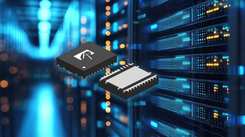
AmpStack packaging.
Why Stack the Die?
A conventional half-bridge built from two discrete DFN5x6 MOSFETs needs two footprints side by side on the PCB, plus copper routing to connect the switch node between them. That routing adds parasitic inductance, and inductance on a fast-switching node shows up as ringing at the switch node and extra voltage stress on the MOSFETs.
AmpStack removes that routing step by placing the two dies vertically in a single package and joining them internally with a clip at the switch node. Because the two dies already share a package, the same PCB footprint that once held one DFN5x6 now holds a full half-bridge.
First AmpStack Device Targets 80 V Applications
The first product based on the packaging platform is the AOPL66801, an 80 V N-channel MOSFET wired internally as a symmetric half-bridge.
Both the high-side and low-side MOSFETs feature a maximum RDS(on) of 2.2 mΩ at a 10 V gate drive. The high-side device supports a continuous drain current of 304 A, while the low-side device is rated for 215 A, reflecting their different thermal operating conditions within the package.
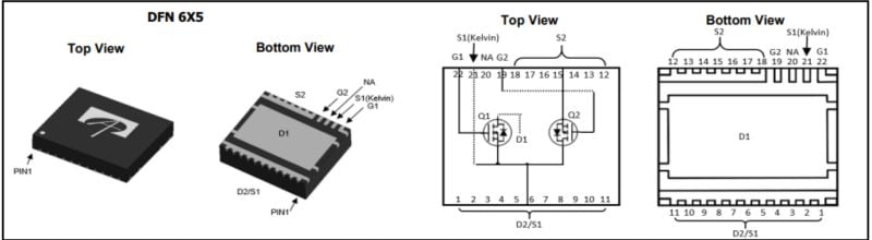
Top and bottom views of the DFN6x5 package.
Addressing Gate-Drive and Thermal Limits
Board layout doesn't just affect the power path. It affects the gate-drive path too. Parasitic inductance in the gate loop can slow switching and add loss, which becomes more of an issue as switching frequency and di/dt rise.
AOS addresses this with a Kelvin sense pin, which is required to keep the gate-to-source voltage stable during fast current transients. The Kelvin connection also gives the high-side gate a more direct drive path, reducing switching losses that would otherwise come from a longer, noisier signal route.
On the thermal side, the part is rated to a 175°C maximum junction temperature, which gives designers more headroom when the package is running at high current density in a smaller footprint than a two-piece discrete solution would occupy.
The AOPL66801 targets power-conversion designs across a wide range of scales, from megawatt-class AI data center power delivery down to motor drives and power tools, and is available now in production.
Full specifications can be sourced from the AOPL66801 datasheet.
What Comes Next
AmpStack is a packaging technology, not a one-off part, and the 80 V AOPL66801 is AOS's first entry rather than the ceiling for what vertical die stacking can do.
As AI server racks push toward higher busbar currents and tighter board real estate at the same time, packaging techniques like this one are becoming a faster path to more power in the same footprint than waiting for the next generation of MOSFET silicon.
All images used courtesy of Alpha & Omega Semiconductor