Facebook
 Google
 GitHub
 Linkedin
Isolation Barrier Stress and Partial Discharge in Gate Drivers
Fast transients can push the gate driver isolation past its normal limits. This can cause partial discharge and, over time, lead to insulation failure in high voltage converters.
In an earlier article, we explored how gate driver failures happen, not just from false turn-on. In high dv/dt systems, repeated transients put extra stress on the isolation barrier in ways that standard voltage ratings do not cover. False turn-on in gate drivers usually shows clear signs, like big fault current spikes and hot spots. But partial discharge damage to the isolation barrier can happen without any warning.
The barrier keeps working, blocking voltage, passing signals, and staying within normal leakage current, even as small internal damage builds up. By the time electrical problems appear, the insulation has already lost much of its useful life. Over time, this causes partial discharge inside the insulation, slowly wearing it down until it fails, even if the system seems to be working within its limits.

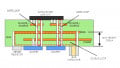
Figure 1. Electrical treeing, branching insulation failure resulting from PD defects, accelerated by high dv/dt switching, leading to eventual breakdown. Image used courtesy of Wikimedia Commons.
Isolation Barriers Under Fast Transient Stress
Gate driver isolation keeps low-voltage control circuits separate from high-voltage switching nodes. Ratings usually focus on steady-state voltage and electric strength, but the real challenge comes from fast-changing electric fields during switching. The voltage across the barrier and the insulation thickness are the two main factors that determine stress. In this case, the average electric field across an isolation barrier of thickness d under a voltage V is:
$$E_{avg} = \frac{v}{d}$$
For example, a digital isolator with a 25 µm polyimide barrier running at 1500 V has an average electric field of 60 MV/m. Polyimides usually handle 200-300 MV/m under direct current, so 60 MV/m gives a good safety margin.
$$E_{avg} = \frac{1500}{25 \times10^{-6}} = 60 \text{ MV/m}$$
However, during transients, if the common mode voltage jumps to 300 V because of switching noise, the electric field rises to 120 MV/m. This is still below the material’s breakdown point, but the safety margin is much smaller.
$$E_{transient} = \frac{3000}{25 \times10^{-6}} = 120 \text{ MV/m}$$
This value is about 40-60% of the material’s breakdown threshold under normal conditions. But real insulation has tiny voids and defects where the electric field is stronger. These spots can see fields 2-5 times higher than the average, so the local field can reach or pass the breakdown point even if the overall field looks safe.
This concentration of stress at defects is why rapid voltage changes (dv/dt) can damage insulation over time, even when staying within rated voltages. After many switching cycles, these transients can eventually break down the insulation.
Transients Voltage Stress vs Rated Isolation
Isolation ratings in data sheets are usually based on steady-state or short tests, like RMS voltage and surge capability. These tests show the barrier can handle certain voltages without breaking down right away. But they do not account for repeated dv/dt stress. When an isolation barrier faces switching transients in a hard-switched SiC converter, the peak voltage includes both the bus voltage and any inductive ringing:
$$V_{peak-transient} = V_{bus} + V_{ring}$$
The ringing can often be 20-50% of the bus voltage. For example, an 800 V bus with 30% ringing results in a peak transient voltage of 1040 V.
$$V_{peak-transient} = 800 + 240 = 1040 \text{ V}_{peak}$$
The equivalent RMS voltage this represents is:
$$V_{RMS} = \frac{V_{peak}}{\sqrt{2}} = \frac{1040}{1.4.14} = \approx 735 \text{ V}_{RMS}$$
But since transients are fast impulses, not smooth waves, their energy and field stress per cycle are not well described by RMS values. Impulse conditions usually trigger PD at lower voltages than AC sinusoidal tests with the same peak. For example, an isolation barrier might pass an AC hi-pot test at 1500 VRMS but fail under repeated 1040 V peak transients. This happens because the high-frequency parts of the impulse waveform focus electrical stress more on material defects than sinusoidal testing does.
In real use, every switching event causes fast electric field changes that are different from standard tests. One key effect is transient amplification. Parasitic capacitance lets transient current flow and common-mode voltage couple into the isolated side. This puts extra stress on the insulation, as displacement currents and local field shifts raise the risk of internal hotspots.
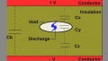
Partial Discharge Mechanism in Gate Drivers
Partial discharge (PD) begins when a strong local electric field is higher than the average field in the insulation, causing ionization in a small area. In high dv/dt converters, PD can happen with every switching cycle, often at the same weak spot. Over time, this wears down the material, causes chemical breakdown, and creates conductive paths. The damage builds up slowly, turning a small defect into a full insulation failure.
Modeling Stress from dv/dt
Isolation barriers always have some parasitic capacitance, so displacement current can flow during fast voltage changes. This current is different from DC leakage:
$$I = C_{iso} \times \frac{dv}{dt}$$
This current is purely transient and gets larger as dv/dt increases. For example, take a gate driver with an isolation capacitance (Ciso) of 2 pF running at a dv/dt of 100 kV/μs.
$$I = C_{iso} \times \frac{dv}{dt} = (2 \times 10^{-12})\times(100\times10^9) = 0.2 \text{ A}$$
This 0.2A flows through the isolation barrier during each transient event. This is important because it causes electric field stress and local heating over time, which speeds up insulation wear even if the driver stays within its normal voltage rating.
Identifying PD in Gate Drivers
You can spot PD in a gate driver in two ways: by watching for electrical signs or by taking measurements. Electrical signs include a slow rise in leakage current across the isolation barrier and high-frequency noise in feedback and control signals during switching. These signs suggest isolation stress, but they do not confirm PD by themselves.
Qualitative Indicators
One sign of PD in gate drivers is a rise in leakage current. If the current stays more than 20% above the starting value, measured at the rated voltage with a precise instrument, it is a good sign of Stage 2 PD. The level of PD, measured in picocoulombs (pC) by IEC 60270 standards, is another way to spot PD in gate drivers. In a gate driver’s isolation system, PD values under 5pC are normal, but values over 10pC show ongoing damage that needs more checking.
In Circuit Detection Limitation
PD detection systems can sense below 1pC in shielded settings, but switching converters make this hard. During normal operation, these converters create broadband electromagnetic noise above 100pC, which hides early PD signals. To monitor PD in active converters, you can use special narrow-band detection systems tuned to frequencies outside the converter’s harmonics, or do regular offline tests in controlled, low-noise conditions.
Why Modern Converters are More Vulnerable
Modern converter designs are more likely to be affected by PD. SiC devices create higher dv/dt, which increases the electric field stress across the isolation barrier. Higher switching frequencies mean more stress cycles every second, which speeds up wear. Compact layouts also focus electric fields near circuit edges and mechanical joints. All these factors put insulation under more frequent and severe stress than older designs.
These factors multiply rather than just add up. For example, compare a basic silicon IGBT converter at 10 kV/μs and 20 kHz to a modern SiC converter at 100 kV/μs and 200 kHz.
| Parameter | SiC IGBT Baseline | SiC Converter | Stress Multiplier |
| dv/dt | 10 kV/μs | 100 kV/μs | 10 x |
| Switching Frequency | 20 kHz | 200 kHz | 10 x |
| Barrier Thickness | 100 μm | 25 μm | 4 x field increase |
| Displacement current (2pF) | 20 mA | 200 mA | 10 x |
Table 1. Cumulative isolation barrier stress comparison between silicon IGBT baseline converter and a modern SiC converter operating within their respective rated voltages.
Not all isolation technologies handle fast transient stress the same way. Their performance depends on how they send signals across barriers and how well their materials deal with rapid electric field changes. These differences affect how easily they are damaged by transient currents, noise, and long-term wear. As dv/dt rises, choosing the right isolation method is key for system reliability. The next article will compare how different isolation technologies perform under this kind of stress.