Facebook
 Google
 GitHub
 Linkedin
Debunking 3 Myths About Aluminum Nitride in Electronics
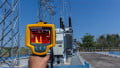
Aluminum nitride is an attractive alternative for next-gen power electronics, such as electric vehicles and renewable energy systems, but myths still surround the compound.
While first developed in 1862, the potential for combining aluminum and nitrogen in electronics was not realized until the 1980s. Several decades later, aluminum nitride (AIN) and its unique properties are seen as ideal for next-generation power electronics, such as renewable energy systems and electric vehicles.
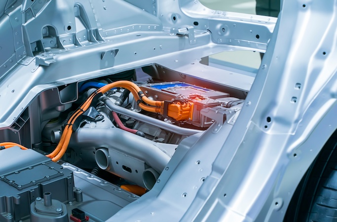
Image used courtesy of Adobe Stock
According to Business Research Insights, AIN is expected to increase its market value annually by 6.9% (CAGR) by 2031, meaning manufacturers are increasing their use of the material for substrates in next-gen products. They will continue to do so over the next decade. An important driver for this demand is the need for efficient thermal management solutions within the power electronics industry, where the increased adoption of electric vehicles and renewable energy systems drive growing demand.
Debunking Aluminum Nitride Myths
As with any advanced material, myths and misconceptions center around aluminum nitride's characteristics and applications:
1. It is expensive to produce.
2. It is difficult to integrate with current manufacturing processes.
3. It is too brittle, especially in substrates with thick copper layers on top and bottom, due to the different thermal expansion coefficients.
Myth 1: AIN is expensive to produce.
Manufacturing costs associated with aluminum nitride are actually on par with other ceramics. AlN is generally less expensive as a raw material than silicon nitride, another material frequently used as a substrate for power electronics.
Prices vary depending on the manufacturing process, material size, packaging, and impurities. There are at least seven elements commonly found as impurities in silicon nitride samples, and they might (or might not) affect the characteristics or behavior of a silicon nitride substrate depending on which are present and at what concentration level. More processing to reduce impurities will, of course, make the material more expensive.
Myth 2: AIN manufacturing processes are inefficient.
A good part of the reason why AlN is being increasingly adopted is that it can be processed relatively easily, using known methods, for multiple purposes.
In power electronics, aluminum nitride is an attractive substrate for many reasons, including its exceedingly high thermal conductivity. AlN substrates can be manufactured using the tape-casting method.
Tape casting is a common technique long used in the low-temperature cofired ceramic (LTCC) process. LTCC involves bonding multiple tapes and pastes (variously conductive, dielectric, and resistive) by laminating them together and firing them in a single step, saving time and money.
For other applications, layers of aluminum nitride can be easily deposited on other materials using chemical vapor deposition (CVD) or physical vapor deposition (PVD).
CVD refers to a group of thermochemical processes in which a precursor material (or materials) in gaseous form is introduced to a sealed chamber containing a heated silicon wafer. Some materials will decompose, while others react with the surface of the wafer. Either way, the desired material will adhere to or be deposited on the wafer. This process is continued until the desired thickness is achieved. CVD has been used in the semiconductor industry for well over 50 years to create a variety of different thin films, including polycrystalline silicon (for transistor gates and interconnect), dielectrics (e.g., silicon dioxide or silicon nitride for transistor isolation), and metals (e.g., copper or tungsten, to connect transistors).
The term PVD also encompasses several techniques, though the mechanics of each are far more varied than the techniques that get the CVD label. They include physical bombardment of the target material (sputtering), ablation (pulse laser deposition), and thermal evaporation (electron-beam evaporation). They have in common that the process involves a solid precursor, which is the key difference from any of the CVD processes. PVD has been used in the semiconductor industry for over 50 years to deposit metallization layers (copper, aluminum), create barrier layers, and under-bump metallization—for connections between the silicon die and package.
These deposition techniques don’t require manufacturers to overhaul their equipment for AIN production, as the material is similar to traditional ceramics.
Myth 3: AIN is a brittle compound.
Military applications are commonly subject to shock and vibration, as are commercial vehicles, including EVs. AIN can indeed fracture without significant deformation in response to stress. This brittleness can pose challenges in specific applications where mechanical strength and toughness are critical, but it is nowhere near brittle enough to overcome its advantages in power electronics. There are mitigation strategies that easily compensate for the drawbacks.
For example, TDK uses tungsten as the conductive material within the substrate; tungsten is a fine conductor and withstands the high sintering temperature used to form AlN substrates. A fundamental property of any material is its melting temperature. TDK sinters its AlN substrates at a temperature over 1800°C. The melting temperature of tungsten is over 3400°C, however, so it withstands the relatively high sintering temperature used to form AlN.
Thin copper layers applied to the top and bottom of the AlN substrate also factor into mechanical strength, but that’s a little more complicated. Generally speaking, the thicker the copper, the better the thermal performance. However, because AlN and copper have different expansion coefficients, thicker copper can lead to delamination or cracks in response to high thermomechanical force as temperatures cycle between extremes.
So, especially in applications such as automotive, where thermal cycling is expected, there’s a tradeoff. Design engineers typically want the thickest layer of copper possible to support the highest possible current density, but that has to be balanced against the imperative from a mechanical standpoint to use the thinnest possible copper layers. So, for every application, engineers must find the sweet spot – the thickness that delivers the best balance between the two considerations.
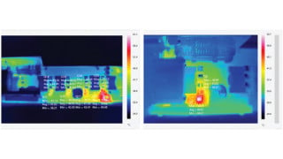
The efficiency with which AlN dissipates heat makes it an attractive alternative to other commonly used ceramic substrates, including Si₃N₄ (silicon nitride) and Al₂O₃ (aluminum oxide). The differences go beyond the efficiency of heat dissipation; they include how heat is dissipated. While traditional ceramic compounds can handle high-temperature dissipation over large surface areas, AIN does so spherically, boosting its efficiency. Moreover, aluminum nitride's thermal capabilities can maintain efficiency in smaller footprints, 5 to 12 times smaller than silicon nitride and aluminum oxide.
Image used courtesy of Adobe Stock
Additional AIN benefits
Aluminum nitride provides many advantages as a substrate material, including being compatible with silicon carbide (SiC) and being ideal for high-voltage power electronics—a combination that takes advantage of the strengths of both materials to provide increased thermal conductivity and electrical insulation. It also bolsters mechanical properties and lowers parasitics like loop inductance and impedance. AlN's thermal expansion coefficient (CTE) is similar to standard silicon, SiC, and gallium nitride (GaN). Therefore, the interconnection between dies and substrate is optimal, and mechanical stress by thermocycling is minimized.
Multilayer aluminum nitride is more versatile than many traditional ceramics. First, the multilayer design allows for tailored properties—balancing factors like thermal conductivity, electrical insulation, and mechanical strength. This adaptability is crucial in power electronics where efficient heat dissipation is paramount.
Additionally, multilayer AlN ceramics can be tailored to customer and OEM requirements, taking power electronics devices to the next technological level. The multilayer architecture will enable devices with higher frequencies and power densities, needed for 800V EV battery architectures, fast-charging charging stations, wind turbines, and solar farms.
Another Option in High-Power Electronics Design
Aluminum nitride substrates represent a promising option in electronics and high-power design. They offer a unique blend of thermal conductivity, electrical insulation, and material compatibility. Multilayer architectures enhance their versatility, allowing manufacturers to produce customer-specific packages and substrates for the semiconductor and power electronics industries. The evolution of innovative manufacturing processes and materials ensures a bright future for AlN substrates, with their potential to revolutionize various electronic devices and offer enhanced performance and efficiency in the evolving landscape of electronics.