Facebook
 Google
 GitHub
 Linkedin
Mitigating Failures in High-Voltage EV Gate Drivers
Explore why high-voltage gate drivers in electric vehicles fail and mitigation strategies for more reliable performance and longevity.
High-voltage gate drivers are crucial in ensuring that power flow in electric vehicles is reliably controlled. From controlling the switching of the inverter's IGBT or MOSFET to monitoring and managing the battery’s state of charge, health, and thermal conditions, high-voltage drivers ensure precise control over switching events. Motor control units and onboard chargers also benefit from these drivers, making them essential to EV functionality. However, these high-voltage drivers are not failsafe.
Let’s examine the failures and how they can be resolved.
Overvoltage and Undervoltage in Gate Drivers
The most common failures are overvoltage and undervoltage. Management is important in ensuring the efficiency and reliability of the EV’s high-voltage gate drivers.
Overvoltage and Mitigation
To understand how to mitigate this issue, we must first explore how overvoltage occurs in gate drivers. During power transistor switching, the high-voltage gate driver responsible for managing power flow in the EV’s electric motor may be subjected to transient spikes because of inductive kickback. When the motor windings are de-energized, the collapse in the magnetic field results in inductive kickback, creating a high spike in voltage. This sudden increase can stress power transistors and gate drivers, leading to failure.
To better break down voltage spike generation, we can evaluate the voltage spike using Lenz’s law by considering the current change rate and the inductive load—in this case, the EV’s motor.
Another cause of overvoltage in high-voltage gate drivers is parasitic inductances resulting from high-speed switching in EV inverter circuits. The voltage overshoot can be approximated by considering the rate at which current changes and the parasitic inductance.
The effects of overvoltage in gate drivers can cause permanent short circuits when the voltage exceeds the switching conductors’ gate oxide breakdown voltage. The magnitude of overvoltage is proportional to the imposed stress on the driver's components. Electromagnetic emissions from high-voltage spikes can interfere with driver efficiency.
Overvoltage can be mitigated with transient voltage suppression (TVS). This involves using semiconductor devices such as TVS diodes that act as voltage clamping devices, which offer the current a low impendence path when the transient current rises above the rated threshold. When selecting a TVS diode for the high-voltage gate driver, consider the peak pulse current that the diode can handle during a transient event and the energy absorbed and dissipated by the diode. Based on the clamping voltage and the transient's power, the TVS diode's current threshold can be easily estimated, where (tpulse) is the transient’s pulse duration.
\[I_{PP}=\frac{E_{transient}}{V_{C}\times t_{pulse}}\]
Another approach to mitigate overvoltage effects in high-voltage gate drivers is using RC snubber circuits, which suppress voltage spikes with resistors and capacitors connected in series. During circuit design, select a capacitor capable of absorbing the energy from the EV’s inductive load to ensure performance. Based on the maximum voltage spike allowable and the inductance and its peak current, an estimation of the capacitance to be used in the snubber circuit can be easily done. On the other hand, selecting the right resistance for the circuit should be based on the characteristic impedance of the circuit, allowing energy dissipation without excessive loss of power.
\[C\geq\frac{L\cdot I^{2}}{V^{2}_{\,\,\,spike}}\]
Undervoltage and Mitigation
Undervoltage is another notable issue that can affect the performance of high-voltage gate drivers in EVs. Inadequate gate driver voltage from undervoltage can lead to incomplete power transistor switching in the driver. This reduces the efficiency of the power conversion process of the drive’s power transistors. Another way Undervoltage impacts gate drivers is by causing switching losses in power transistors through slower switching speeds. Switching losses reduce the switching efficiency of the transistors in the drive by increasing the amount of energy dissipated during a switching event. The switching time (tsw), the drain current (Ids), the switching frequency (fsw), and the drain-source voltage (Vds) can be considered when evaluating the switching loss for more optimized switching characteristics of the power transistors in the EV’s gate drivers.
\[P_{sw}=\frac{1}{2}V_{ds}\times I_{ds}\times f_{sw}\times t_{sw}\]
When mitigating undervoltage, two common approaches can be taken to optimize the performance of the gate drivers. The first uses an Undervoltage lockout (UVLO) that maintains a minimum voltage threshold by monitoring the voltage supply. If there is a drop in the supply voltage below the minimum threshold, the driver is disabled to avoid inadequate operation. UVLO threshold sums up the minimum voltage needed for a complete switching of gate transistors and a set safety margin that accounts for aspects like noise, tolerance, and voltage drop in the UVLO circuit.
The second approach uses power switching and linear regulators like low dropout (LDO). These supply voltage regulators ensure adequate power transistor switching and power loss reduction in the gate drivers. The regulators often use two resistors to form a voltage divider in which the resistor ratio determines the output voltage after regulation. In the internal reference circuit of the voltage regulator, we can also consider its reference voltage (Vref) to evaluate the regulated supply voltage. This is essential when designing a gate driver’s power supply for a more precise and stable power flow, helping maintain the overall performance and reliability of EV powertrains.
\[V_{out}=V_{ref}\Big(1+\frac{R_{2}}{R_{1}}\Big)\]
Thermal Stress in High-Voltage Gate Drivers
Manifesting through thermal cycling and overheating, thermal stress occurs when the cooling capacity of the gate drivers and their switching transistors is exceeded. High-voltage gate driver overheating results from high switching frequencies where each switching event introduces losses that generate heat. Inefficient thermal management techniques also contribute to overheating in high-voltage gate drivers.
During the design process, the cooling systems are often limited by space, resulting in poor ventilation or bad heatsink design. This makes the heat generated poorly dissipated, leading to the degradation of the driver’s semiconductors and mechanical stress due to thermal expansion. When excess heat degrades semiconductor material, the scattering of charge carriers increases within the semiconductor lattice, increasing the switching device's on-state resistance. This increases conduction losses and causes thermal runaway, leading to failure if not properly mitigated. Thermal cycling, on the other hand, occurs when there is a variation in load conditions. In this case, the high-voltage gate drivers may be subjected to thermal cycling through frequent stop-start operations instead of steady-speed driving that keeps the EV power demand steady.
Thermal stress can be mitigated by optimizing the cooling system design. When designing a heatsink, it is essential to account for thermal resistance (θja), ensuring it is low enough to keep the junction temperature (TJ) within safe levels. By considering the total power dissipated by a power transistor, the junction temperature can be evaluated to achieve a reliable heatsink design. A larger fan and efficient ventilation combined with an efficient heatsink design, can greatly mitigate thermal stress in the gate drivers.
\[T_{j}=T_{a}+P_{total}\times\theta_{ja}\]
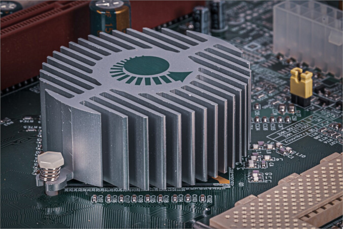
Figure 1. Heatsink design for thermal stress management. Image used courtesy of Pixabay
Higher junction temperatures in power transistors used in high voltage gate drivers can cause conduction losses resulting from increased on-state resistance of the transistors. This leads to reliability concerns such as accelerated aging of the semiconductor material and eventual failure from electromigration and oxide breakdown.
Reliable High-Voltage Gate Drivers
A reliable high-voltage gate driver ensures stable and efficient power control in EVs. With the growth in EV technology, mitigating common failures in the driver becomes essential for longevity and optimized performance. Engineers can, therefore, draw insight into some of the common ways failures can be mitigated for a reliable gate driver design.