Facebook
 Google
 GitHub
 Linkedin
GaN-Based Synchronous CCM PFC for Hydraulic Pump Power Supply Applications
This article details a GaN-based synchronous CCM-PFC design for hydraulic pump power supplies. It achieves 98.5% peak efficiency at 300W and operates without a heatsink, solving common condensation issues in industrial applications.
Article co-authored by STMicroelectronics’ Giuseppe D’Agata.
This article is published by EEPower as part of an exclusive digital content partnership with Bodo’s Power Systems.
This article describes the final GaN-based design of a synchronous CCM-PFC without heatsink. A real prototype has been realized and optimized by using a GaN system-in-package and a dedicated controller. Comparison with the Si-based version of the same system shows that GaN allows to reach up to 300 W maximum load, with a 98.5 % peak efficiency. Consequently, the GaN switches can operate at a safe low temperature, avoiding overheating even if no heatsink has been used like in conventional PFC solutions.
Power supplies for industrial three-phase motor drivers often require a pre-regulator power factor correction (PFC) to reduce input current distortion and ensure compliance with harmonic content regulations. State-of-the-art solutions typically use simple out-of-phase correctors to achieve near-unity power factor at the cost of significant harmonic distortion and power losses.
Active PFC regulators minimize total harmonic distortion (THD) and improve overall efficiency. Residual power losses are usually dissipated through heatsinks, but these are unsuitable for applications such as hydraulic pumps. In such cases, the heatsink is cooled by the liquid flow drained by the pump, leading to condensation issues due to temperature differences between the liquid and the pump body. Therefore, in this market segment, efficient and heatsink-less designs with high power density are in high demand. To address these challenges, a GaN-based continuous conduction mode (CCM) boost pre-regulator PFC offers a viable solution by minimizing power losses and eliminating the need for heatsinks.
For this purpose, a 300 W European range synchronous PFC prototype was developed using a power GaN System-in-Package [1], achieving high power factor and low THD. This result was also obtained thanks to a dedicated controller [2], which senses the inductor current using a shunt resistor placed on the GND return current path.
Main Specifications and System Description
The main characteristics of the synchronous CCM-PFC boost converter prototype board are as follows:
- Input voltage: 230 VAC, 50Hz nominal (185-265 VAC, 45-65 Hz range)
- Regulated output voltage (VOUT): 400 VDC
- Rated output power (POUT_MAX): 300 W
- Input current distortion (THD): < 10 % from full load to 20 % load
- Power Factor (PF): > 0.9 from full load to 20 % load
- Converter peak efficiency (η): 98 %
- Switching frequency (FSW): 65 kHz
- Mains harmonics: meets EN61000-3-2 Class-D and JEITA-MITI Class-D
- EMI: according to EN55022 Class-B
- PCB: double-sided, 70 µm, FR-4
Figure 1 illustrates the evaluation board prototype, composed of a motherboard and a daughter board hosted through a dedicated connector. The motherboard includes an input common-mode EMI filter, a bridge rectifier, and a dedicated boost inductor designed for CCM applications up to 300 W. As in standard PFC designs, a low-value input capacitor and an output bulk capacitor complete the boost frame.
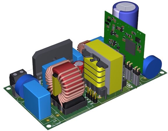
Figure 1. Evaluation board prototype, composed of a motherboard and a daughter board hosted through a dedicated connector. Image used courtesy of Bodo’s Power Systems [PDF]
The PFC operates in CCM at full load, enabled by the dedicated controller. It can also function in DCM or boundary conduction mode, facilitated by the ZCD circuitry.
The daughter board, shown in Figure 2, embeds the core of the PFC and can be considered composed of three main blocks:
- GaN-based half-bridge with an onboard VCC supply.
- Control logic, generating two complementary driving signals starting from the PFC controller one, and adding an adjustable dead time.
- High-speed, low-consumption comparator to detect current zero crossing. Together with the previous one, this block allows to keep the high side in forward conduction as long as possible. This enhances efficiency by preventing negative inductor current and thus energy backflow.
Additional daughter board features include self-start-up logic, operating before the PFC controller turns on, and ZCD compatibility with transition-mode PFC. A dedicated PCB has been designed with a compact form factor while ensuring adequate heat dissipation, especially for the low side on which most of the heat is generated. For this reason, a larger copper area and 30 thermal vias have been put near its exposed pad. PCB design optimization details are available in [3].
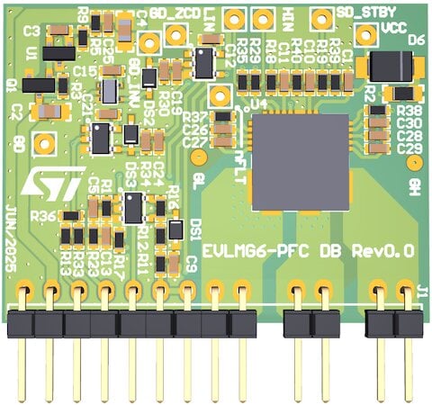
Figure 2. This daughterboard for the evaluation board embeds the core of the PFC. Image used courtesy of Bodo’s Power Systems [PDF]
Experimental Results
The following waveforms show the operation of the synchronous PFC at light (Figure 3a) and full load (Figure 3b). Note that the inductor current is always positive even when the load is decreasing.
The details of the switching operation near the sinusoid peak and zero crossing are shown in Figure 4a and Figure 4b, respectively.
Even at light load, the ZCD comparator is working properly, allowing the DCM operation as shown in Figure 5a and Figure 5b. The proper system operation ensured a unity power factor and low THD.
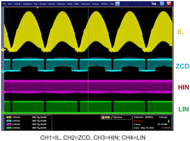
Image used courtesy of Bodo’s Power Systems [PDF]
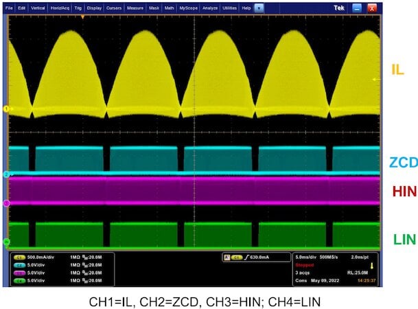
Figure 3. Operation of the synchronous PFC at light (3a) and full load (3b). Image used courtesy of Bodo’s Power Systems [PDF]
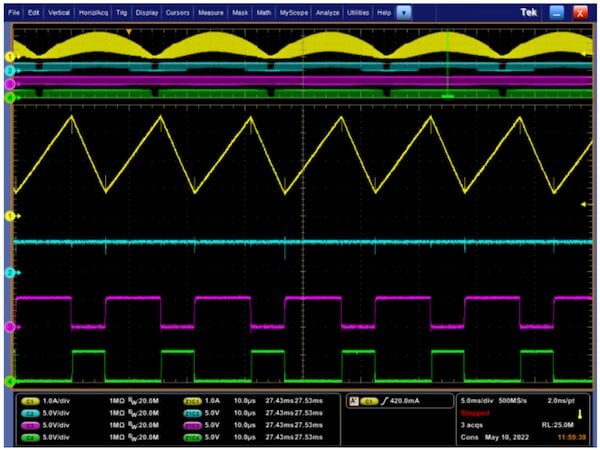
Image used courtesy of Bodo’s Power Systems [PDF]
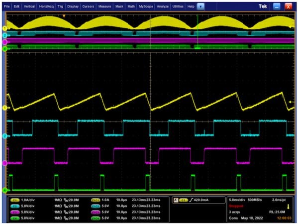
Figure 4. Switching operation near sinusoidal peak (4a) and zero crossing (4b). Image used courtesy of Bodo’s Power Systems [PDF]
Table 1. Efficiency measurements – Si MOSFET + SiC diode versus GaN HB comparison.
|
FSW [kHz] |
RS [Ω] |
∆LM [%] |
LM [mH] |
VIN [VAC] |
IOUT [A] |
VOUT [V] |
POUT [W] |
PIN [W] |
Eff. [%] |
TAMB [°C] |
TC [°C] |
|
Si MOSFET + SiC diode |
|||||||||||
|
65 |
0,22 |
30 |
1,8 |
230 |
0,495 |
401,50 |
198,74 |
203,57 |
97,6 |
25 |
75 |
|
65 |
0,22 |
30 |
1,8 |
230 |
0,614 |
401,90 |
246,77 |
254,54 |
96,9 |
25 |
85 |
|
GaN half bridge |
|||||||||||
|
65 |
0,22 |
30 |
1,8 |
230 |
0,493 |
401,92 |
198,15 |
202,55 |
97,8 |
25 |
53 |
|
65 |
0,22 |
30 |
1,8 |
230 |
0,596 |
401,93 |
239,55 |
245,15 |
97,7 |
25 |
57 |
|
65 |
0,22 |
30 |
1,8 |
230 |
0,700 |
398,90 |
279,23 |
285,77 |
97,7 |
25 |
64 |
Table 2. Efficiency measurements with GaN half bridge – 130 kHz vs 65 kHz.
|
FSW [kHz] |
RS [Ω] |
∆LM [%] |
LM [mH] |
VIN [VAC] |
lOUT [A] |
VOUT [V] |
POUT [W] |
PIN [W] |
Eff. [%] |
TAMB [°C] |
TC [°C] |
|
130 kHz |
|||||||||||
|
130 |
0,1 |
60 |
0,929 |
230 |
0,503 |
399,40 |
200,90 |
205,76 |
97,6 |
25 |
77 |
|
130 |
0,1 |
60 |
0,929 |
230 |
0,623 |
399,30 |
248,76 |
254,36 |
97,8 |
25 |
90 |
|
130 |
0,1 |
60 |
0,929 |
230 |
0,698 |
399,20 |
278,64 |
285,44 |
97,6 |
25 |
99 |
|
65 kHz |
|||||||||||
|
65 |
0,1 |
60 |
0,929 |
185 |
0,504 |
399,80 |
201,50 |
207,30 |
97,2 |
25 |
66 |
|
65 |
0,1 |
60 |
0,929 |
230 |
0,500 |
399,50 |
199,75 |
203,28 |
98,3 |
25 |
48 |
|
65 |
0,1 |
60 |
0,929 |
230 |
0,760 |
399,75 |
303,81 |
308,51 |
98,5 |
25 |
63 |
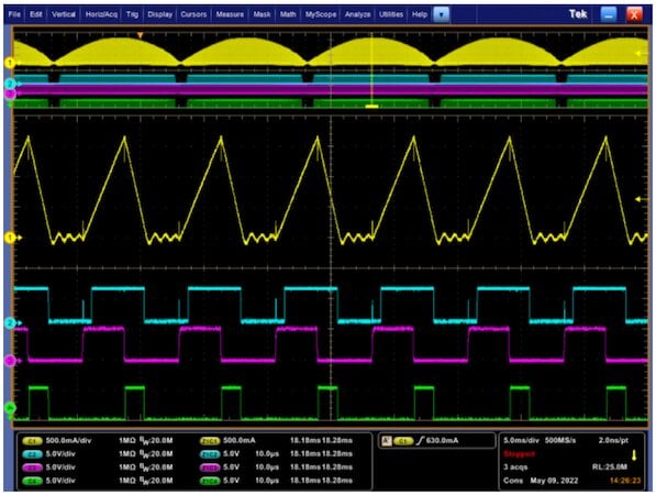
Image used courtesy of Bodo’s Power Systems [PDF]
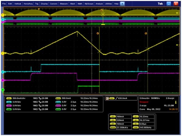
Figure 5. DCM operation at light load. Image used courtesy of Bodo’s Power Systems [PDF]
Efficiency Measurements and Comparison with Conventional Solutions
The initial prototype was designed with the typical parameters and sizing of a traditional CCM PFC operating at 65 kHz. The design was tested using a silicon MOSFET as a low-side and a SiC diode for high-side rectification. A second test has then been performed under identical conditions, using the GaN half-bridge without a heatsink. The GaN and Si MOSFET RDS(on) were similar for a fair comparison.
Efficiency measurements and thermal behavior data were collected and are reported in Table 1. These preliminary findings indicate that the GaN-based synchronous solution enables a more efficient design with higher output power.
The final design was optimized by using a lower inductor value, allowing the converter to operate predominantly in DCM with limited CCM operation. A lower sense resistor was selected to mitigate dynamic limitations and enhance overall efficiency. This final version was tested by running it both at 130 kHz and 65 kHz, comparing performance and efficiency in each case. As Table 2 shows, the second case allows for higher output power and overall efficiency.
References
[1] “High power density 600V Half bridge driver with two enhancement mode GaN HEMT” MasterGaN6 datasheet. (See www.st.com)
[2] “CCM PFC controller with high voltage startup” L4985 datasheet, DS13769. (See www.st.com)
[3] AN5917: “PCB design optimization for maximizing thermal dissipation in MASTERGAN Family” (See www.st.com)
[4] Levati, F. (2020, September). Testing GaN HEMT Performance in High Power Factor Solutions. In 2020 AEIT International Annual Conference (AEIT) (pp. 1-6). IEEE. the high side
This article originally appeared in Bodo’s Power Systems [PDF] magazine.