Facebook
 Google
 GitHub
 Linkedin
Designing High-Voltage SiC-Based Battery Disconnect Switches
When designing a high-voltage solid-state battery disconnect switch, there are several fundamental design decisions to consider.
This article is published by EEPower as part of an exclusive digital content partnership with Bodo’s Power Systems.
Electrical systems with DC bus voltages of 400 V or greater, powered by single- or three-phase grid power or an energy storage system (ESS), can enhance their reliability and resilience with solid-state circuit protection. When designing a high-voltage solid-state battery disconnect switch, there are several fundamental design decisions to consider. Among the key factors are semiconductor technology, device type, thermal packaging, device ruggedness, and managing the inductive energy during circuit interruption. This article addresses design considerations in selecting the power semiconductor technology and defining the semiconductor packaging for a high-voltage, high-current battery disconnect switch, as well as the importance of characterizing a system’s parasitic inductance and over-current protection limits.
Advantages of Wide-Bandgap Semiconductor Technology
Careful consideration is required to select the optimal semiconductor material to realize a switch with minimal on-state resistance, minimal off-state leakage current, high voltage-blocking capability, and high power capability. Figure 1 shows semiconductor material characteristics for Silicon (Si), Silicon Carbide (SiC), and Gallium Nitride (GaN). The electric breakdown field of SiC and GaN is approximately ten times that of silicon. This enables the design of devices with a drift region that is one-tenth the thickness of an equivalent rated silicon device since its thickness is inversely proportional to the electric breakdown field. Moreover, the resistance of the drift region is inversely proportional to the cube of the breakdown field. This results in nearly 1000 times lower drift region resistance. In a solid-state switch application, where all the losses are conduction losses, the high electric breakdown field is a significant advantage. This decreased resistance also eliminates concerns with dynamic latch-up issues, where high dV/dt transients may trigger the parasitic NPN transistor or thyristor in silicon power MOSFETs and IGBTs, respectively.
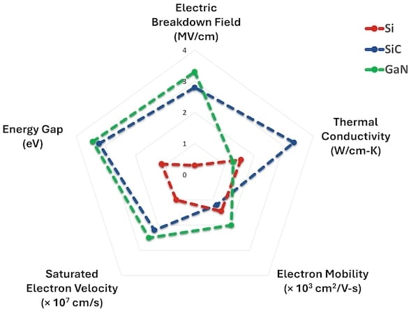
Figure 1. Si, SiC, and GaN material properties. Image used courtesy of Bodo’s Power Systems [PDF]
Silicon carbide’s thermal conductivity, three times that of Si and GaN, significantly improves the ability to draw the heat out of the chip, enabling it to run cooler and simplifying the thermal design. Alternatively, for an equivalent target junction temperature, it allows higher current operation. The higher thermal conductivity, coupled with the high electric breakdown field, results in a low on-resistance, further simplifying the thermal design.
Silicon carbide, a wide-bandgap (WBG) semiconductor material, has an energy gap nearly three times that of silicon, which enables higher-temperature operation. A semiconductor ceases to function as a semiconductor at elevated temperatures. The wider energy gap allows silicon carbide to operate several hundred degrees Celsius higher than silicon since the concentration of free charge carriers is lower. However, other factors (e.g., packaging, gate oxide leakage) based on today’s technology limit a device’s maximum continuous junction temperature to 175°C. Another advantage of WBG technology is it provides a lower off-state leakage current.
Considering these characteristics, silicon carbide is the optimal semiconductor material for this application.
Differences Between IGBTs, MOSFETs, and JFETs
The type of transistor is the next critical factor. In most cases, the conduction loss presents the greatest design challenge. The conduction loss should be minimized to meet the system’s thermal requirements. Liquid cooling is available in some systems, while others may use forced air or rely on natural convection. In addition to minimal conduction loss, the voltage drop must also be kept to a minimum to maximize efficiency across all operating points, including light-load conditions. This is especially important in battery-powered systems. Another important factor in many systems, including DC systems, is bi-directional current flow. A transistor with low conduction loss, low voltage drop and reverse conduction capability is generally desired. Transistors typically considered are IGBTs, MOSFETs, and JFETs.
While an IGBT offers comparable conduction loss as a MOSFET at peak load currents, once the load current decreases, the efficiency of an IGBT-based solution decreases. This is because the voltage drop is comprised of two components: a near-constant voltage drop that is independent of the collector current and a voltage drop that is proportional to the collector current. With a MOSFET, the voltage drop is proportional to the source current. It does not have the overhead of an IGBT, and this enables high efficiency across all operating points, including light-load conditions. The MOSFET allows channel conduction in the first and third quadrants, meaning current can flow through the device in the forward and reverse direction. An added benefit of a MOSFET’s third-quadrant operation is that it generally has a slightly lower on-state resistance than in the first quadrant. Whereas, an IGBT conducts current only in the first quadrant, and an anti-parallel diode is needed for reverse current conduction. The JFET, an older technology but making a resurgence, works in both forward and reverse conduction, and, like the MOSFET, has a voltage drop proportional to the drain current. Where it differs from a MOSFET is it is a depletion-mode device. That is, the JFET is normally on and requires a gate bias to inhibit the flow of current. This presents practical challenges for designers when considering system fault conditions. As a workaround, a cascade configuration that includes a series of low-voltage silicon MOSFETs can be used to realize a normally-off device. The addition of the series silicon device increases the complexity, which diminishes some of the advantages of the JFET in high-current applications. The SiC MOSFET, a normally-off device, offers the low resistance and controllability needed in many systems.
Thermal Packaging
SiC power modules enable a high level of system optimization that is difficult to realize with paralleling discrete MOSFETs. Microchip’s mSiC modules are available in a range of configurations and voltage and current ratings. Among these is the common-source configuration that connects two SiC MOSFETs in an anti-series configuration to allow bidirectional voltage- and current-blocking. Each of the MOSFETs is composed of multiple chips connected in parallel to achieve the rated current and low on-state resistance. For a unidirectional battery disconnect switch, the two MOSFETs are connected in parallel externally to the power module.
A low on-state resistance and low thermal resistance are needed to keep the chips running cool. The materials used within the module are essential elements that determine the thermal resistance from junction to case, as well as its reliability. Specifically, the die-attach, substrate, and baseplate material properties are the major contributors to a module’s thermal resistance. Selecting materials that exhibit high thermal conductivity helps minimize the thermal resistance and junction temperature. In addition to thermal performance, selecting materials with closely matched Coefficient of Thermal Expansion (CTE) increases the module’s lifetime by reducing the thermal stress at both the interface and the interior of the materials. Table 1 summarizes these thermal characteristics. Aluminum Nitride (AlN) substrates and Copper (Cu) baseplates are standard in mSiC power modules. Options with Silicon Nitride (Si3N4) substrates and Aluminum Silicon Carbide (AlSiC) baseplates provide higher reliability. In Figure 2 are common-source power modules in the standard SP3F and SP6C packages and high-reliability baseplate-less BL1 and BL3 packages which are qualified for DO-160.
Table 1. Die, substrate, and baseplate thermal properties.
| Material |
CTE (ppm/K) |
Thermal Conductivity (W/cm-K) |
Density (g/cm3) |
|
| Die |
Si SiC |
4 2.6 |
136 270 |
|
| Substrate |
Al2O3 AlN Si3N4 |
7 5 3 |
25 170 60 |
|
| Baseplate |
CuW AlSiC Cu |
6.5 7 17 |
190 170 390 |
17 2.9 8.9 |
Device Ruggedness and System Inductance
Along with a module’s thermal performance and long-term reliability, another design consideration in a circuit interruption device is the high inductive energy. Relays and contactors have a limited number of cycles. They are commonly specified with unloaded mechanical switching cycles and significantly fewer electrically-loaded switching cycles. Inductance in the system results in arcing across the contacts, causing degradation when a current is broken. As such, the operating conditions of the electrical cycle rating are specifically defined and have a strong influence on its life. Even then, upstream fuses are needed in systems with contactors or relays, as the contacts may weld shut when subjected to high short-circuit currents. Solid-state battery disconnect switches do not suffer from this degradation, enabling a higher reliability system. Despite that, understanding the parasitic and load inductance and capacitance of a system is also essential in managing the inductive energy present when interrupting high currents.
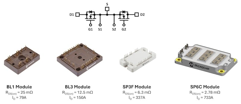
Figure 2. Microchip’s mSiC modules in common-source configuration. Image used courtesy of Bodo’s Power Systems [PDF]
The inductive energy is proportional to the inductance and to the square of the current in the system at the time of interruption. A short circuit at the output terminals of the switch results in a fast increase in current, rising at a rate of the ratio of the battery voltage to the source inductance. As an example, an 800 V bus voltage with 5-microhenry source inductance results in the current increasing at a rate of 160 A per microsecond. A 5-microsecond response time to detect and respond will result in an additional current of 800 A in the circuit. As it is not recommended to operate a SiC power module in avalanche mode, a snubber or clamp circuit is required to protect the module by absorbing this inductive energy. However, the parasitics introduced to the snubber circuit, when properly designed to meet creepage and clearance requirements, further limit its effectiveness. Therefore, the switch should turn off slowly enough to limit the voltage overstress from the module’s internal inductance and the sudden decrease in its current. A module designed with low inductance helps further minimize this voltage stress.
In silicon power devices, a fast interruption of a high current introduces the risk of triggering the parasitic NPN or thyristor, which results in an uncontrollable latch-up and eventual failure. On SiC devices a very fast turn-off may result in a low-energy avalanche breakdown in each chip as they turn off until the snubber or clamp absorbs the high energy. Microchip’s mSiC MOSFETs are designed and tested for Unclamped Inductive Switching (UIS) ruggedness, providing an additional safety margin as a snubber or clamp begins to degrade. Figure 3 shows the single-shot and repetitive UIS performance compared with other SiC devices in the market.
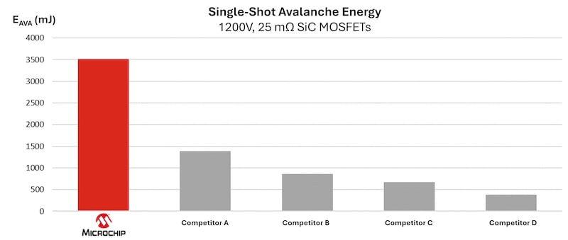
Image used courtesy of Bodo’s Power Systems [PDF]
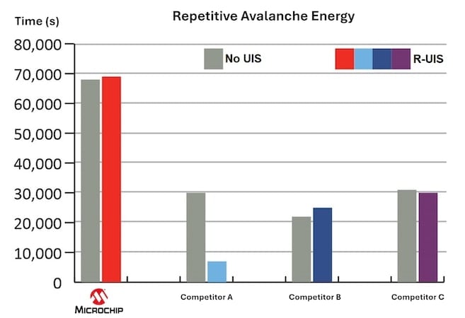
Figure 3. Single-shot (top) and repetitive (bottom) avalanche energy performance. Image used courtesy of Bodo’s Power Systems [PDF]
Although device-level short circuit capability should be understood, and IGBTs do have superior device-level short-circuit performance over MOSFETs, in an actual system it is subjected to different stress conditions. With the inherent current-limiting behavior of the system inductance, a module is unlikely to reach its short-circuit current rating. The limiting factor is the snubber or clamp circuit design. To design a cost-effective and compact snubber, the allowable system-level peak short-circuit current will be limited to a value well below a module’s short-circuit current rating. For example, in a 500 A battery disconnect switch consisting of nine parallel chips designed to prevent short-circuit currents from exceeding 1350 A, each chip conducts a current of 150 A, assuming uniform current distribution. This is a much lower current than in a device-level short-circuit test in which the current exceeds several hundred Amps for the duration of the test. Optimization of the voltage clamping device is a key part of the design of a robust solid-state battery disconnect switch.
Other Design Considerations
Beyond the power device, there are design considerations related to the control electronics, including current sensing technology, overcurrent detection and protection, and functional safety. Decisions on whether to use a shunt resistor or magnetic technology for current sensing are important for a design in a system with low parasitic inductance, where a fast response time is essential. Whether to use hardware, software, or a combination of the two for over-current detection is also an important decision, especially when designing to meet functional safety requirements. The advantages of silicon carbide and power semiconductor packaging are key enablers to the system-level benefits a solid-state disconnect switch offers over the traditional mechanical disconnect switch. Using silicon carbide technology, devices are now available with low on-state resistance and thermal resistance, allowing the low conduction loss needed in many systems while also using materials that ensure high reliability.
This article originally appeared in Bodo’s Power Systems [PDF] magazine.
Related Content