Facebook
 Google
 GitHub
 Linkedin
Silicon Carbide Current-Limiting Devices
This article highlights the drawbacks, advantages, and features of silicon carbide current-limiting devices.
A known justification for Electrical Protection is to prevent transitory event like lightning, EMI, short-circuit, as well as transitory power-up effects, from disturbing and possibly permanently damage impacted electronic systems.
Most frequent design approach to Electrical Protection is voltage clamping devices (TVS, MOV, GDT) together with current limiting ones (fuses, resistors, polymeric PTC, inductors). Figure 1 shows a typical schematic of fast surge protection for fast surges combining voltage clamping and current limiting devices mentioned above

Figure 1: Typical surge protection schematic.
For specific applications, like aircraft lightning protections, tripping speed, reliability, and failure mode concerns prevent the use of MOV and GDT. This drives aircraft lightning protection designs to use almost exclusively TVS-only structures. To pass Aircraft Lightning Protection Test [1] require sizing up TVS to bulky devices which has a cost impact.

Figure 2: Clamping voltages on a TVS for two current values.
In other cases, standard current limiting devices can be used together with voltage clamping devices.
The following table summarizes the drawbacks of standard current-limiting devices.
| Standard Current Limiting Devices | Drawbacks |
| Resistors |
|
| PPTC |
|
| Inductors/Chokes |
|
| Silicon Devices |
|
The next section introduces Silicon Carbide Current Limiting Devices. Such innovative Silicon Carbide Current Limiting Device (SiC CLD) brings advantages summarized in the following table.
| Advantages of SiC CLD | Features |
| Fast reaction time | <100nsec |
| Self-resettable behavior | No external action required |
| Low nominal resistance | From hundred mΩ |
| High dynamic resistance | Up to several hundred Ω |
| No Disconnection | Protected circuit always ON |
| Small footprint | SMB (DO-214AA) |
| High transient-voltage capability | Above 1600V |
| Extreme reliability and robustness | 1000’s operations without degradation |
| Wide bandwidth | DC to multi GHz |
SiC Current Limiting Device in a Nutshell
A Silicon Carbide Current Limiting component is a two-terminal device. When the CLD voltage drop is greater than its threshold voltage, the device clamps the current going through it to a specific value. This maximum current value is set by its internal topology. As shown in Figure 3, SiC CLDs behaves like a current source in DC. When CLD voltage is below saturation voltage VSat, the CLD behaves like a resistor which value is ROn. Above this voltage VSat, the CLD current saturates at ISat value. Thus, SiC CLDs can be considered as semiconductor non-linear resistors.

Figure 3: Typical DC behavior of a SiC CLD.
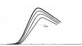
In dynamic behavior, the current through CLDs decrease as the junction temperature increases. This is due to self-heating (i.e. junction power dissipation) which increases the equivalent CLD resistance (Figure 4). This resistance increase limits the current inside the device and constrains the self-heating. Therefore, by default, the device remains in a safe area of operation. Figure 9 shows the dynamic response of a typical SiC CLD to a short square pulse.

Figure 4: Typical dynamic response of a SiC CLD.
SiC CLDs are described by four principal parameters:
- ROn: ON-state resistance
- ISat: saturation current
- INom_Max: Maximum nominal current before saturation
- VMax: maximum use voltage before breakdown
CLD design took care to comply with 1.2/50μs from IEC 61000-4-2, 40/120μs from DO-160 section 22 making CLD a remarkable fit to it. To ease design with CLD datasheet provides a simple-to-use accurate Safe Operating Area (SOA) graph to assess the quick suitability of the CLD device to a specific application. To manage the CLD electrothermal performances a SPICE simulation model is available (Figure 5). More information can be found at application notes of [2].

Figure 5: Model of a SiC CLD and measured and simulated dynamic response to a normalized 1000V/1000A, 8-20μs waveform.
Multiple Flavors of SiC CLD
SiC CLDs are either unidirectional or bidirectional (see Figure 6). A bidirectional CLD clamps both positive and negative current

Figure 6: Unidirectional and bidirectional behavior, with corresponding device symbols.
Application benefits of SiC CLDs
SiC CLDs are well suited for many different types of applications such as (Figure 7):
lightning protection on data or power supply lines,
- reduction of inrush current during start-up of converters,
- protection of sensitive equipment against line transients,
- protection of submarine cable communication repeaters against cable short circuits.

Figure 7: SiC CLD applications in different markets.
SiC CLD is a current-clamping device that is dual to a voltage clamping device such as MOV, TVS or GDT. Combining both in a π (Pi) topology protection circuit ends up with a very compact solution (Figure 8).
In common practice, a resistor is implemented in between the GDT and the TVS. The purpose of this resistor is to protect the TVS against current surges. At the same time, this resistor value has to be as low as possible to limit the power dissipation in normal operation. SiC CLDs supplies a new response to deal with this dilemma thanks to its non-linear resistor characteristics. In nominal conditions, SiC CLDs presents a low resistance, and this one highly increases when the voltage across the device is high due to a surge condition. This allows using low-power rating TVS, which in turn reduces system footprint and cost. Additionally, for communication lines, SiC CLDs offer lower insertion losses than the needed equivalent resistor, presenting also virtually zero parasitic inductance.

Figure 8: Pi-configuration protection circuit.

Figure 9: Measured dynamic response (blue) of a SiC CLD (KE12LEB150T20 bidirectional mode) to a normalized 900V/900A, 1.2-50μs waveform (red).

Figure 10: Measured insertion loss S21.
Speed and Safety
Exhibiting very low parasitic inductance and taking advantage of the SiC material properties, SiC CLD is ideal for ultra-fast current clamp-ing while sustaining high energy. Perfect Fast and safe!

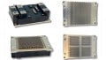
Figure 11: Caly’s SiC CLD Packaging options.

Figure 12: Full set of evaluation boards for SiC CLD assessment.
Figure 9 shows Off-The-Shelf SiC CLD (KE12LEB150) real-time dynamic response to a normalized 900V/900A 1.2-50μs lightning waveform. At the beginning of the waveform, current through the SiC CLD is clamped almost instantaneously (50-100ns) to ISat and then it drops quickly per device self-heating.
As mentioned in previous sections, SiC CLD is a perfect fit to high-speed data communication line protection. It brings wide bandwidth performance whilst current clamping is still ensured. Off-The-Shelf SiC CLD insertion losses (S21) up to 4.5GHz is shown in Figure 10.
What Does a CLD Look Like?
Depending upon the intended use and targeted market, SiC CLDs are available in diverse forms and packages. Package selection must consider DC power dissipation as much as required AC characteristics. Multiple choices are available to you to fit your need in package size and application requirements.
To facilitate your CLD experimentation various flavors of demo boards are awaiting your call.
References
[1] "Environmental Conditions and Test Procedures for Airborne Equipment", RTCA/DO-160G, RTCA Inc. December 16, 2014
[2] Improving Performance of Surge Protection Circuits with Current Limiting Devices
About the Author
Dr. Jean-Baptiste Fonder (FAE) received his Electrical Engineering degree at ENSEA, masters degree in the Field of Electronic of Autonomous Systems and Doctor of Philosophy in Electrical Engineering at University of Cergy-Pontoise, and Post Doctoral Researcher of "Failure analysis on wide bandgap d evices" at University of Rouen and then Silicon Carbide (SiC) power devices characterization at National Institute of Applied Sciences of Lyon. He is working as a Field Application Engineer at CALY Technologies.
Dr. Dominique Tournier (CTO) works as the Chief Technical Officer (CTO) at CALY Technologies. He received his PhD degree from the Institut National des Sciences Appliquées (INSA), Lyon, France, in 2003. From 2005 until 2015, he was Associate Professor at Ampère-Laboratory (INSA Lyon). His interests and developments were in SiC device design and fabrication for high power electronics applications and functions integration for high-temperature electronics. He has supervised 4 PhD theses and has authored and co-authored more than 120 research papers in journals and conferences mostly on SiC devices and applications. He also holds 7 patents mostly focused on protection devices and systems.
Gonzalo Picun (BDM) received his Electrical Engineering degree in the field of Microelectronics at University of the Republic, and Master of Science in the field of High-Temperature Microelectronics at Catholic University of Louvain. He worked as a business development manager at CALY Technologies.
Laurent Martinez (Sales Mgr) worked as a Sales Manager at CALY Technologies.
Related Content