Facebook
 Google
 GitHub
 Linkedin
The Creation of Silicon Carbide Revolutionary Semiconductor
This article highlights SiCrystal AG and Rohm Semiconductor GmbH for the potential of Silicon Carbide material for power and RF electronics applications.
Compared to silicon or gallium arsenide, the Silicon carbide (SiC) is a rather young base material in the semiconductor industry but its origins date back to the end of the 19th century. In 1891, Edward Acheson developed a method for producing crystalline SiC as an abrasive material — a method still in use today. During this same time, French chemist H. Moissan conducted the first mineralogical studies of the “second-hardest mineral occurring in nature.” Because of this, SiC is sometimes called Moissanite today.
When the semiconductor age began in the middle of the 20th century with the introduction of the bipolar transistor, the enormous potential of silicon carbide for specific applications was already understood. According to the discoveries of E. Johnson, the product of breakdown field strength and saturation drift velocity may be used as an indication of a material’s suitability as a base material for transistors in RF and power applications. In this comparison, SiC turns out to be much better than both silicon and gallium arsenide.
In practical applications, however, the innovative semiconductor material was unable to prove its superiority immediately, because no process able to produce sufficiently large silicon carbide substrates with the low defect rates required to manufacture meaningful test structures existed at that time. The Acheson process and the so-called Lely process are the intermediate steps in developing the production of SiC substrates but it was the modified Lely process that provided the basis for the modern production of SiC substrates in the late 1970s. When better and larger silicon carbide substrates became available thanks to the evolution of this basic process, SiC provided a completely convincing performance.
Production Prerequisites for Silicon Carbide
Before the production (which is called ‘growth’ by experts) of a silicon carbide crystal can begin, the essential components for the production of a silicon carbide crystal must be in place, including the crystal growth equipment itself, the growth process, various media, the source material, and the seed crystal.
The source material, silicon carbide, acts as a raw material in the growth process and continuously feeds the growing crystal. The source material is normally in powder form, and is produced in a preceding process. This preceding process is a strictly controlled high-temperature process combining the base materials which are highly pure silicon and carbon. Precise control ensures that base material is used which is characterized by a specific, internally specified purity, stoichiometry, grain size, grain distribution, and other internally defined specified parameters.
The seed crystal is a mono-crystalline, round silicon carbide slice that initiates (and largely controls) the growth of a large mono-crystal, hence the term ‘seed’. Like the seed of a plant, the seed crystal imparts significant ‘genetic information’ to the growing crystal. The structural perfection of the seed crystal determines much of the crystal’s optimum absence of defects and its durability. The multi-stage selection process used by our company continuously ensures that seed crystals will only be made of the best in-house crystals featuring optimum material quality. The constant internal selection serves as a distillery process that continuously improves the quality of the seed and the final product.
The Significance of the Seed Crystal as Confinement to Silicon Crystals Growth
The crystal growth equipment, the growth process, the media, the source material, and the seed crystal (silicon included) play a significant role in the processes used for producing other semiconductors with the exception of silicon carbide. Explained in more detail in the section below, the SiC crystals are grown through a special vapor-phase process. For this reason, the diameter of the seed crystal should have at least the target diameter of the crystal to be grown. With silicon (Figure 1), it is not possible to grow a large crystal of sufficient quality on a seed rod with a relatively small diameter. Any defects in the seed would be ‘inherited’ by the growing crystal due to the ‘genetics’ described above, mandating the use of a flawless, large-diameter seed crystal for silicon carbide.

Figure 1: Significance of the Seed Crystal for Growing Si and SiC Crystals
Therefore, the seed crystals are among the factors supporting the secure operation of the enterprise. Not commercially available anywhere, this material acts as a kind of copy protection. Securely protected by internal processes, it is always available in sufficient quantity at SiCrystal.
The Growth of the Silicon Carbide Crystal
When all the required conditions described above are met, the growth process itself can begin. The sublimation growth method is usually used for SiC. The setup then consists of a graphite crucible, which is surrounded by carbon-based insulation material. This helps to save energy and is inserted into the induction-heated growth equipment (see Figure 2). The crystal growth process then proceeds in the following manner:
The induction coil of the growth equipment induces circular currents in the graphite growth crucible, heating it up to well over 2273 K. At these elevated temperatures, the source material in the lower zone of the crucible evaporates and the silicon carbide powder sublimes, turning into various gaseous species. The gases consist of silicon and/or carbon which fill up the free space of the crucible.
Although they are still above 2273K, the seed crystal attached to the top of the crucible does not evaporate because temperatures are lower there.
Adhering to the laws of thermodynamics, the gaseous species formed by the source material at temperatures far above 2273 K have the tendency to deposit from the vapor phase when they are transported close to the colder seed crystal. Crystallizing on the surface of the seed, they form additional crystal volume and let the crystal grow. These crystals do not grow in an uncontrolled manner, however, because the ‘genetics’ of the seed predicts the growth with a crystallographic relationship to the seed.
A doping material — normally gaseous nitrogen — is intentionally added in the vapor phase during the crystal growth. The dopant electrically acts as a donor ensuring the intended conductivity of the crystal and is incorporated into the crystal in a low and well-defined quantity,
The growth process, therefore, relies on the constant transfer of material from the source to the growing crystal. The growth process, which requires the continuous transport of species and dopant through the vapor phase, lasts a couple of days. When the powder has almost completely evaporated and a crystal of several centimeters in length has grown, the process is terminated in a controlled manner.

Figure 2: SiC Crystal Growth Process
There are several other aspects which enable the process in the way described above. Both the crucible and its insulation are made of carbon. The carbon lends itself to this purpose because of its high-temperature stability, its availability in semiconductor purity and the fact that it does not represent an elementary contamination for SiC. All the carbon parts would immediately burn at 2273 K under normal atmospheric conditions, so it is necessary to run the process in an inert atmosphere (argon is often used). To contain all gases including the argon, the crucible and its insulation are surrounded by two coaxial glass tubes whose intermediate space is cooled with water.
Manufacturing Silicon Carbide Substrates: The Wafer-Production Process Chain
At the final stage of the crystal growth process, a cylindrical single crystal of several centimeters in length, whose diameter is larger than the target diameter, can be taken from the crucible. The subsequent process steps are almost identical to other established semiconductors, including silicon. The main steps include:
- Crystal orientation using x-ray analysis
- Cylindrical grinding of the crystal to the desired diameter
- Grinding of flats (markings on the crystal surface)
- Sawing wafers from the crystal
- Application of individual laser markings for wafer identification
- Rounding off the edges of the wafers
- Surface treatment with methods including
- Grinding
- Lapping
- Polishing by mechanical abrasion
- Polishing by chemical/mechanical abrasion
- Cleaning the wafers using dry or wet chemical methods
As a matter of course, these process steps are accompanied by checking many internally- or externally-specified parameters using special optical, mechanical, chemical and electrical methods. The large amount of data acquired and archived ensures full traceability of the final product back even to the raw material batch used in the initial process stage.
The process described above is long established as the standard in manufacturing semiconductor substrates. The process stages, processing facilities, and inspection methods are basically known from silicon processing. Nonetheless, processes and/or machines sometimes had to be modified to accommodate the specific properties of silicon carbide.
On the Mohs’ hardness scale, where diamonds represent the upper limit with a hardness of 10 and all minerals are considered very hard with hardness values greater than 6, SiC is among the top scorers with a hardness of 9 which is considered a very hard material. Only a few materials are available for the abrasive machining of silicon carbide. The tools and process equipment must be adapted to reliably provide semiconductor customers the required product precision.
Challenges and Solutions to the Growth Process and Wafer Production
The key challenges in the production of silicon carbide crystals and substrates is ensuring the highest quality based on ever-tightening specifications. In this context, quality means the quality of the wafer surface:
- Absence of scratches
- Extremely low, nanometer-scale surface roughness
- Surface purity in a physical sense (particles, films) and in an electrical sense (electrically active impurities)
- In addition, it also means geometrical quality:
- Tight diameter and thickness tolerances
- Minimum bow and warp of substrates
- Exactly specified edge shape
Also, to a high degree, it means internal or better intrinsic quality:
- Homogeneity of the doping and thus the conductivity
- Stresses in the material that are as low as possible
- The low density of dislocations or related defects
Today’s State of the Art SiC Quality
Although quality naturally is a ‘fast-moving target’, it is justified to say that SiC fully meets the customer’s requirements for an established semiconductor material today. However, much work was required in the past to reach and maintain this level.
Comparing the ‘old’ and current substrates using stress birefringence method reveals that there is an enormous improvement in material quality in the last 15 years or so. Stress birefringence is an optical method representing deviations from the ideal state as white areas, while undisturbed regions are displayed as black areas shown in Figure 3.

Figure 3: Diameter increase and quality improvement
Strong contrasts are visible on the entire surface of the wafer from the year 2000 shown on the left-hand side of Figure 3, indicating defect-related stress. Responsible defects include dislocations and related structural defects, proving that the growth process was not sufficiently optimized in the year 2000.
The current state of the art shown on the right-hand side of Figure 3 is quite different. Although the sensitivity of the optical method has improved a lot in the meantime, there are almost no contrasts between dark and bright areas. This clearly indicates that the growth process was optimized significantly, that the defect density within the crystal has been reduced by several orders of magnitude and that current wafers are production-worthy without any limitation.
But how can these improvements of material quality be achieved? In this case, these quality improvements were achieved by an optimization of the crystal-growth process. But how can one optimize a high-temperature process operating at temperatures far above 2273 Kelvin Placing sensors in the crucible area is hardly conceivable at these elevated temperatures. Furthermore, any additional ‘observation hole’ in the insulation for optical temperature measurements from the outside would unacceptably influence the temperature distribution within the crucible. The growth process would corrupt if there is any macroscopic opening in the growth crucible, because that opening would inevitably lead to the escape of process gases.
As shown in Figure 4, the problem can be solved by numerically simulating the growth of the crystal. Using special software and considering all relevant material and process parameters, crystal growth experts now can ‘look into the crucible’.

Figure 4: Temperature distribution in the crystal growth crucible
Experienced crystal growers can adequately recognize from the temperature distribution (the so-called thermal field) how a crystal would grow under modified growth conditions (Figure 4). Through this, a multitude of ‘numerical experiments’ will limit the number of necessary ‘real experiments’. The combinations of simulation with experimental confirmation have enabled crystal growers with many years of experience to achieve the radical improvement of material quality described above.
Wafer Surface Quality Improvements
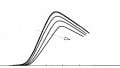
The above-mentioned comparison between the current product and the wafer from the year 2000 revealed the diameter increase from 35mm to 150mm. At present, the wafers feature a significant quality improvement on a wafer surface which has increased by a factor of 18. This trend towards increased wafer size accompanied by continuously improving quality will continue as the most important goal in the future. Predominantly as larger wafer surfaces can be processed more economically, thereby lowering production costs.

Figure 5: Evolution of SiC wafer diameters
The transition from 100mm to 150mm is just beginning for today’s customers. There will be an interesting transition in the possible introduction of the 200mm substrate as the next stage of evolution. Although it may take some time for this next step to become commercially viable, SiCrystal expects to be able to deliver the first samples within two or three years.
Summary
Although the potential of silicon carbide for power and RF electronics applications has been recognized quite early, a suitable manufacturing process for this material was only developed by the end of the 1970’s. In the industrial process used until today, the original SiC material sublimes before being transported through the vapor phase and crystallizing on a SiC seed crystal. This creates a single crystal, which is subsequently processed into substrates using modified process stages long established in the semiconductor industry.
The continuously increasing requirements regarding the quality and diameter of the substrates were and are considered by process adaptations based on computer simulation. Thanks to their high-quality level, today’s substrates with diameters of up to 150mm can be used for component production without limitation. Optimally positioned for the present and the future, the ROHM subsidiary SiCrystal is prepared for the journey towards larger diameters and further improved quality.
About SiCrystal AG
SiCrystal AG is among the world’s leading manufacturers of silicon carbide semiconductor substrates. Founded in 1996 and headquartered in Nuremberg, Germany, the wholly-owned subsidiary of ROHM CO. LTD delivers its products to customers all over the world.
The company owns all processing stages from the production of the original material to packaging the epi-ready substrate in an in-house clean-room environment. In addition to the results of its comprehensive, proprietary analysis methods, SiCrystal AG has direct access to the results of component tests within the ROHM Group. This is an invaluable benefit for advancing the material optimization based on component or even module performance.
About the Authors
Dr. Robert Eckstein studied materials science at the Friedrich-Alexander-University Erlangen-Nuremberg and obtained his doctorate in 1998 on the subject of crystal growing of silicon carbide. He has been working for SiCrystal AG since 1997 where he holds the position of CEO. He is responsible for development, production and sales.
Aly Mashaly completed his studies in electrical engineering at the University of Cairo, followed by a master's program at the Leibniz University Hannover. He started his career as a Development Engineer Power electronics at Liebherr Elektronik GmbH. He then took over the management of the eMobility division at KEB GmbH. He has been working for Rohm Semiconductor GmbH since July 2015, where he is responsible for the Power Systems division for the European market.
This article originally appeared in the Bodo’s Power Systems magazine.
Related Content