Facebook
 Google
 GitHub
 Linkedin
Reengineering Silicon Power Devices for High-Efficiency Conversion
Reengineering silicon power devices with new architectures overcomes material limits to achieve significantly higher efficiency and power density.
Silicon power MOSFETs have served as the backbone of power conversion systems for decades, offering a well-balanced combination of performance, cost, and manufacturability across a wide range of applications. From point-of-load converters to motor drives and battery systems, silicon has remained the dominant technology due to its maturity and scalability.
However, as efficiency requirements tighten and power density targets continue to rise, a prevailing narrative has emerged suggesting that silicon has reached its fundamental limits. This perspective reflects silicon’s intrinsic material limits, yet recent innovations in device architecture and process technology have pushed performance beyond what those limits were once thought to allow.
For more than two decades, progress in silicon power devices has been driven primarily by incremental process improvements rather than fundamental structural innovation. As a result, many of the long-standing tradeoffs between conduction losses, switching performance, and voltage capability have remained largely unchanged.
A new generation of silicon device architectures is now challenging this assumption by reengineering how electric fields and charge are managed within the device. These innovations demonstrate that silicon still has significant untapped potential when approached from a fundamentally different design perspective.
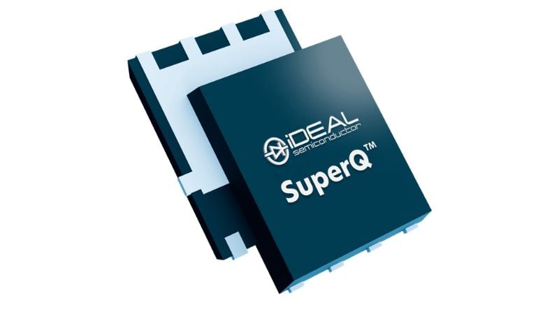
The SuperQ silicon MOSFET.
The Efficiency Wall in Conventional Silicon MOSFETs
Silicon MOSFET performance is governed by the relationship between breakdown voltage and specific on-resistance (RSP). In traditional one-dimensional device structures, this relationship follows a well-known scaling law in which RSP increases approximately with the breakdown voltage raised to the power of 2.5 (BV2.5).
This behavior is driven by the need for a thicker and more lightly doped drift region to sustain higher voltages. While necessary for voltage blocking, this region contributes significantly to conduction losses, making higher-voltage devices inherently less efficient.
The introduction of RESURF-based Superjunction architectures represented a major step forward by enabling two-dimensional charge balancing within the drift region. This allowed RSP to scale toward a more favorable linear relationship with breakdown voltage. However, even these architectures introduce structural limitations. In Superjunction devices, only a portion of the device cross-section actively conducts current, while the remainder is dedicated to voltage blocking.
As a result, the symmetrical p- and n-pillar structure constrains conduction efficiency, and further improvements require increasingly complex and costly manufacturing processes. In practical terms, these limitations define an efficiency ceiling for conventional silicon MOSFETs.
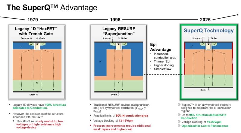
Figure 1: Cross-sectional drawings of legacy 1D, Superjunction, and SuperQ MOSFETS
Reengineering Silicon Through Advanced Electric Field Control
iDEAL Semiconductors' SuperQ technology fundamentally rethinks how silicon devices manage electric fields and charge distribution. Rather than relying on symmetrical charge balance structures, this new approach introduces asymmetrical RESURF architectures (as shown in Figure 1) that significantly improve conduction efficiency while maintaining high-voltage capability.
In these architectures, a deep, high-aspect-ratio trench containing controlled charge replaces the traditional Superjunction p-pillar. This trench occupies only a small fraction of the device area, on the order of up to a few percent, while most of the cross-section remains available for current conduction.
This structural change dramatically increases the effective conduction area, allowing up to approximately 95% of the device cross-section to contribute to current flow. At the same time, precise charge balance is maintained across the drift region, enabling robust voltage blocking through two- and three-dimensional electric field control.
The result is a more uniform electric field distribution, reduced field crowding, and improved tolerance to process variations. These factors collectively enable higher doping concentrations in the drift region without compromising breakdown voltage.
Surpassing Traditional Limits in Specific On-Resistance
One of the most significant outcomes of the SuperQ architecture is the ability to break through the conventional limits of specific on-resistance for a given breakdown voltage. By enabling a thinner, more heavily doped drift region while maintaining charge balance, these devices achieve substantially lower RSP than both conventional silicon and Superjunction technologies.
Measured results demonstrate that SuperQ power MOSFETs can deliver reductions in on-resistance ranging from approximately 1.6× to 5.7× compared to legacy silicon devices in the 150 V to 400 V range, as shown in Figure 2. In addition, the enhanced electric field control supports field strengths on the order of 19–20 V/µm, representing a significant improvement over conventional Superjunction designs.
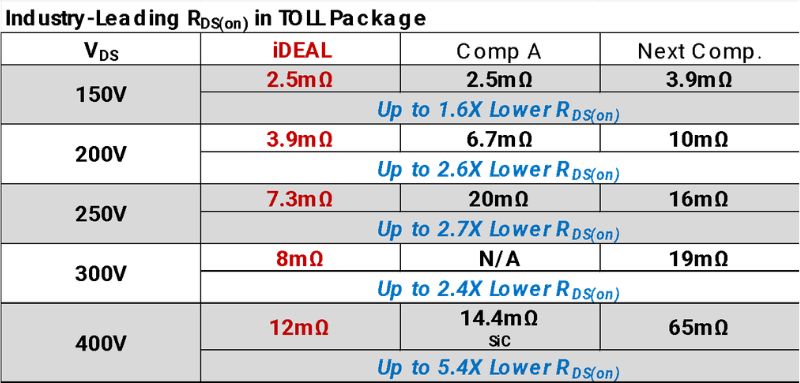
Figure 2: Comparison of RDS(on) for SuperQ MOSFETs at various voltages vs traditional silicon MOSFETs
These improvements directly translate into lower conduction losses and enable industry-leading resistance in a package, improving both efficiency and cost-performance metrics. The combination of improved efficiency and manufacturing simplicity yields a more favorable cost-to-performance ratio, reinforcing silicon’s competitiveness in high-volume applications.
Decoupling Conduction and Switching Losses
Inherent tradeoffs between conduction and switching performance have long governed power MOSFET design. Reducing on-resistance typically requires increasing device area or modifying the structure in ways that increase capacitance. This leads to higher gate charge, output charge, and switching losses.
Conversely, optimizing for fast switching often results in higher conduction losses or increased susceptibility to electromagnetic interference due to higher dv/dt and di/dt. These competing constraints create a tightly coupled design space in which improvements in one parameter degrade another.
SuperQ power MOSFETs challenge this long-standing relationship by optimizing charge distribution and minimizing parasitic capacitances through structural innovation rather than simple scaling.
As a result, these devices can achieve lower total switching charge and reduced energy per switching event, improving efficiency at practical operating frequencies. This is particularly important in applications operating in the 100 kHz to several hundred kilohertz range, where switching losses often dominate the overall loss profile. By simultaneously improving both conduction and switching performance, SuperQ MOSFETs effectively decouple two of the most restrictive trade-offs in power device design.
System-Level Implications for Efficiency and Power Density
The benefits of improved device performance extend directly to the system level. Even relatively small increases in efficiency can significantly reduce thermal dissipation, enabling smaller heatsinks and simplified cooling strategies. Lower junction temperatures also contribute to improved reliability and longer system lifetimes.
In battery management systems, lower conduction losses reduce heat generation and improve system reliability, especially in high-current environments. In motor drive applications, low on-resistance enables higher power and greater ruggedness in the inverter.
In DC-DC conversion, operating at higher switching frequencies enables smaller magnetics and faster transient response. This leads to higher power density and more compact system designs, which are increasingly important in applications with space and weight constraints. The cumulative effect of these improvements is a more efficient, compact, and cost-effective power conversion system.
Maintaining the Advantages of the Silicon Ecosystem
A key advantage of SuperQ innovation is its compatibility with established manufacturing processes and supply chains. Unlike wide bandgap technologies, which often introduce the additional cost of specialized gate drivers, the added design complexity of non-standard gate voltages and tighter layout constraints, and require new fabrication methods and materials, SuperQ devices can be produced using CMOS-compatible processes with high yield and scalability, leveraging existing infrastructure and high-volume production.
Compared to traditional Superjunction processes, which can be complex and capital-intensive, these newer architectures require relatively modest process steps.
From a reliability perspective, these devices maintain the robustness associated with silicon, including strong safe operating area (SOA) characteristics, industry-leading short-circuit withstand capability (SCWC), and proven qualification to industry standards such as AEC-Q101.
This allows manufacturers to leverage existing infrastructure while delivering improved performance, reducing both cost and supply chain risk. For system designers, this translates into a lower barrier to adoption and greater confidence in long-term availability and reliability.
Conclusion: Redefining What Silicon Can Achieve
The notion that silicon has reached its limits largely reflects the constraints imposed by conventional device architectures rather than the material itself. For more than two decades, designers have operated within the tradeoffs defined by symmetrical RESURF structures and incremental process improvements.
By fundamentally reengineering how electric fields and charge are managed within the device, new silicon architectures are overcoming these long-standing limitations. The resulting improvements in specific on-resistance, switching performance, and robustness demonstrate that silicon remains well-suited to meet the demands of modern power conversion systems.
Rather than being displaced, silicon is being innovated. These advances provide a path to higher efficiency and power density while preserving the cost, manufacturability, and reliability advantages that have made silicon the dominant technology in power electronics.