Facebook
 Google
 GitHub
 Linkedin
Advancing Industrial Power Conversion With Silicon Carbide
This article explores the benefits of SiC devices in selected use cases, including HVAC systems, DC fast charging infrastructure, and solar and energy storage systems.
This article is published by EEPower as part of an exclusive digital content partnership with Bodo’s Power Systems.

Image used courtesy of Adobe Stock
Silicon carbide (SiC) has emerged as one of the most transformative wide-bandgap (WBG) semiconductor technologies in power electronics. SiC MOSFETs and SiC diodes certainly outperform conventional silicon-based devices. Higher breakdown voltages, faster switching speeds, far greater efficiency under real operating conditions – these properties enable designers to build better power conversion systems that are more compact, thermally robust, and energy-efficient across the entire load range.
Industrial applications such as heating, ventilation, and air conditioning (HVAC), electric vehicle (EV) DC fast charging systems, photovoltaic (PV) inverters, and energy storage solutions (ESS) are increasingly adopting SiC technology. The driver is not only performance but also regulatory and market demand for higher efficiency, smaller form factors, and reduced lifecycle cost.
SiC in HVAC Systems
HVAC systems are rapidly adopting SiC not only for its performance advantages but also in response to new regulations and growing market demands for greater efficiency, smaller form factors, and lower operational costs.
SiC technology addresses these needs in two critical parts of the system - motor inverters and power factor correction (PFC) stages (see Figure 1).
Motor Inverters
In conventional motor inverters of HVAC systems, silicon IGBTs still dominate. However, their switching losses and limited efficiency at partial loads constrain overall system performance.
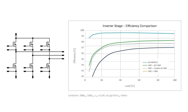
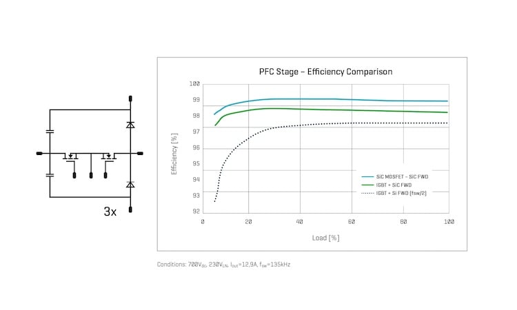
Figure 1. SiC showing clear efficiency advantages, especially under light-load operation in the motor inverter (top) and PFC (bottom) stage. Image used courtesy of Bodo’s Power Systems [PDF]
Replacing them with SiC MOSFETs results in:
- Greater efficiency across the load profile: SiC’s lower conduction and switching losses improve efficiency not only at full load but also during partial load conditions, which dominate in typical HVAC mission profile
- Reduced audible noise: Operating at higher frequencies in range of 16 to 20 kHz shifts inverter-induced noise out of the audible spectrum
- Lower operating costs: Although SiC devices have a higher upfront cost, the energy savings over the system’s lifetime deliver a superior cost-performance ratio
SiC MOSFETs offer significant efficiency advantages in motor inverter applications, especially under partial-load conditions. Unlike IGBTs, which maintain a fixed saturation voltage regardless of current, SiC MOSFETs exhibit resistive behavior, allowing conduction losses to scale down proportionally with load current. This makes them inherently more efficient at low operating currents, where the constant voltage drop of IGBTs becomes a dominant loss factor.
These benefits can be further enhanced in embedded drive systems that integrate the inverter and motor into one unit. In such configurations, long motor cables are eliminated, and motor windings are typically designed with insulation rated for higher dv/dt levels. This enables SiC devices to operate at higher dv/dt slew rates using relatively low gate resistor values to further reduce switching losses and improve efficiencies, also at upper load conditions.
On the other hand, in standard industrial motor drives the dv/dt slew rates often need to be limited to around 5 kV/µs to protect winding insulation in motors and reduce electromagnetic interference (EMI). To meet this requirement, designers typically choose between two approaches: increasing the gate resistor (Rg) to slow down the dv/dt of SiC MOSFETs, or maintaining relatively low gate resistance and adding an external dv/dt filter.
Using high Rg values restricts the switching performance of SiC devices and leads to increased switching losses, which may require a larger heatsink volume to manage the additional thermal dissipation. In contrast, a dv/dt filter keeps switching losses low, but requires additional filtering components. [1]
PFC Converters
Figure 1 clearly illustrates how SiC technology outperforms IGBTs in a state-of-the-art neutral boost PFC (NPFC) topology. By using SiC components, the switching frequency is increased to around 135 kHz, close to the conducted EMC level of 150 kHz, where the pure Si solution operates at half that switching frequency. Already the change of FWD by SiC brings efficiency gain from 97,6 to 98,4 % at nominal load. The efficiency can exceed 99 % by replacing IGBTs with SiC MOSFETs.
Opting for SiC components in the PFC stage has multiple benefits:
- Compact PFC design: Higher switching frequencies minimize the size of passive components, enabling more compact designs
- Greater efficiency than Si, even at higher switching frequencies
- Lower system costs: Smaller magnetic components, heat sinks, and enclosures reduce overall system costs
- SiC diodes as a key enabler: Their zero reverse recovery loss is essential for achieving both high efficiency and high-power density. IGBTs with SiC diodes are the more cost-effective solution, while a full SiC delivers superior performance.
However, in the PFC stage, topology selection plays a decisive role in determining overall system cost and performance trade-off. The following chart benchmarks and compares four topologies under consistent operating conditions.
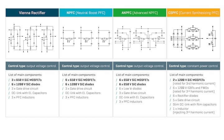
Figure 2. State-of-the-art 3-phase PFC topologies and novel CSPFC topology. Image used courtesy of Bodo’s Power Systems [PDF]
The first three topologies in Figure 2 are voltage source converters with output voltage control capability. Although they require a similar number of gate drive circuits, PFC inductors, and large electrolytic DC-link capacitors, the Vienna topology uses a single SiC MOSFET per phase, while in NPFC and ANPFC, the SiC MOSFETs are in a back-to-back configuration.
In the ANPFC topology [2], which is Vincotech’s proprietary topology, it is possible to reduce the breakdown voltage of the boost diodes from 1200 V to 650 V, enabling the use of less pricey, lower-voltage SiC FWDs.
The Current Synthesizing PFC topology in Figure 3 is based on 3rd harmonic current injection and requires constant power control. The advantages of this topology are that it reduces the SiC content in circuits, calls for just one inductor for 3rd harmonic injection rather than three PFC inductors, and does not need large electrolytic DC link capacitors [3].
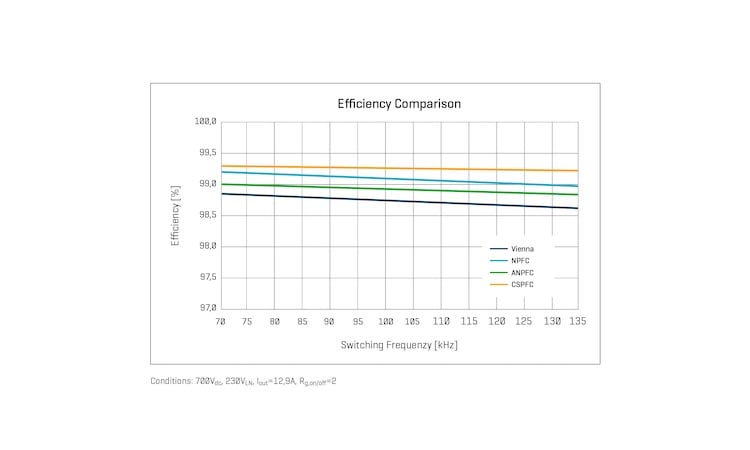
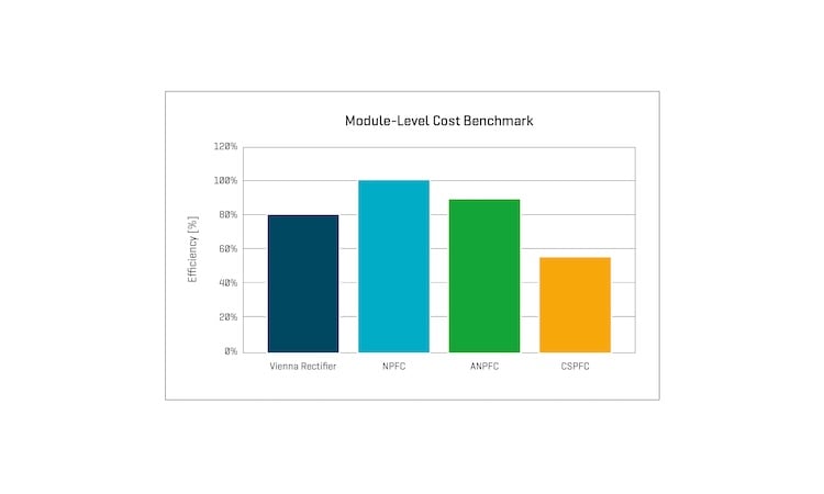
Figure 3. Efficiency and module-level cost benchmark of three-phase PFC topologies. Image used courtesy of Bodo’s Power Systems [PDF]
An efficiency benchmark reveals that the NPFC topology achieves the highest efficiency among voltage source converters, but also has the highest costs driven by the extensive use of SiC components.
The advanced neutral boost PFC (ANPFC) topology offers a cost reduction of approximately 10 %. This is achieved by lowering the breakdown voltage of the boost diodes from 1200 V to 650 V, allowing the use of more cost-effective components. However, due to the higher voltage drop across two series-connected diodes during freewheeling, the efficiency is approximately 0.2 % lower compared to the NPFC topology.
Further cost savings of around 10 % can be realized with the Vienna rectifier, which uses only one SiC MOSFET per phase. However, due to higher losses in MOSFETs, it also results the lowest efficiency.
The 3rd harmonic injecting CSPFC topology shows the highest efficiency. Here, the SiC MOSFETs can easily switch at high switching frequencies, as they have only to switch the 3rd harmonic current. However, the disadvantage of this topology is the lack of output voltage regulation, which can only be realized by adding an additional DC/ DC stage. As the SiC content in this topology is minimal, it also offers the lowest costs.
SiC in EV Charging Infrastructure
In the DC fast charging infrastructure, SiC has already established itself as a core technology. Its widespread adoption is driven by the growing demand for faster, more efficient, and scalable charging solutions. SiC enables significant improvements in system efficiency - boosting it from typical levels around 95 % to as high as 98 % - while offering better compatibility with higher battery voltages of 800 V and above.
Beyond efficiency gains, SiC contributes to lower operating costs and enables smaller installation footprints. Both of these benefits are crucial for public charging infrastructure, where space and accessibility are key.
Figure 4 shows several topologies for AC/DC and isolated DC/DC converters. Depending on the output power and battery voltage range, one topology or the other can offer a better cost-performance ratio. However, there are clear trends and a narrower choice for bidirectional charging coming from the vehicle-to-grid (V2G) use case. In this scenario, electric vehicles not only take power from the grid, but can also feed energy back into it.
This capability helps to stabilise the grid, supports the integration of renewable energy, and enables EVs to act as mobile energy storage during times of peak demand or outages.
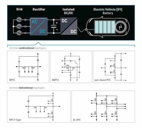
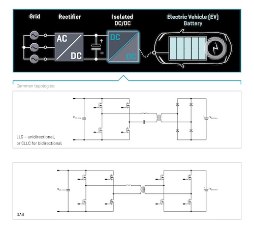
Figure 4. State-of-the-art uni- and bidirectional topologies in DC fast charging for AC-DC and DC-DC power conversion. Image used courtesy of Bodo’s Power Systems [PDF]
Towards Megawatt Charging
Megawatt charging systems (MCS) are fast becoming a necessity for long-haul, heavy-duty vehicles such as trucks and buses. These systems can deliver up to 3.75 megawatts. Able to stay on the road longer with fewer pit stops, vehicles operate more efficiently.
Today’s MCSs mainly reuse infrastructure for fast charging systems (CCS), achieving higher power levels by stacking multiple subunits, designed for battery voltages up to 920 V. However, the next generation of MCSs is shifting toward 1250 V battery voltages, making integration with 1500 V DC-coupled systems – common in renewable energy and energy storage systems – much simpler.
In this architecture, centralized PFC stages or solid-state transformers (SSTs) can connect directly to the medium-voltage grid, followed by modular DC/DC converters. This setup relies heavily on SiC’s ability to operate at higher voltages and switching frequencies while maintaining system efficiency. It also requires power modules equipped with the new voltage class of SiC MOSFETs rated for 2 kV or higher.
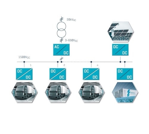
Figure 5. System architecture example of a megawatt charging system. Image used courtesy of Bodo’s Power Systems [PDF]
SiC in PV Inverters and ESS
In the residential and commercial PV inverter markets, the use of SiC technology is growing rapidly, especially in hybrid inverters that integrate both solar and battery charging functionalities into a single unit. However, the largest share of SiC deployment is from utility-scale string inverters and energy storage systems.
Hybrid topologies combining conventional Si with SiC components are a popular choice for such use cases. These solutions balance cost and performance. For one, they use SiC where its benefits are most impactful, such as in power modules’ high-frequency parts. For the other, they retain Si in low-frequency parts where its performance suffices and comes at a lower cost.
Boost Stage for PV Inverters
PV inverters typically use two-stage power conversion, where DC/ DC boost converters take care of maximum power point tracking (MPPT) and adjust the PV panel output voltage to the required DClink voltage level. That is the input for DC/AC inverters, which feed solar energy into the public grid. In this input stage, two-level and three-level symmetric boost topologies are commonly used, but newer designs are exploring three-level flying capacitor boost architectures [4] for high-power, utility-scale applications.
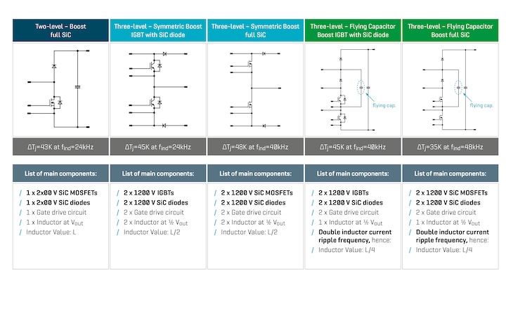
Figure 6. Commonly used boost converter topologies in PV applications, with the list of main components and the main chip junction temperature (Tj ) increase at recommended switching frequencies. Image used courtesy of Bodo’s Power Systems [PDF]
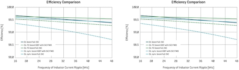
Figure 7. Efficiency and cost benchmark of boost converter topologies under the same inductor current ripple frequency. Image used courtesy of Bodo’s Power Systems [PDF]
Two-level boost converters are simpler, but they require higher-voltage SiC components of 2kV or more. On one hand, to provide sufficient breakdown voltage margin above the 1500 V dc-link and to ensure cosmic ray robustness, and on the other hand, to meet the efficiency target.
However, these components are significantly more expensive than 1200 V devices used in three-level topologies. Additionally, due to thermal constraints, more chips must be paralleled. As voltage increases, MOSFETs also switch more slowly, so their use is recommended for lower switching frequencies below 24 kHz, resulting in larger and heavier boost inductor needs.
Three-level topologies introduce an additional third voltage level. This reduces the voltage across the boost inductor. Consequently, for a given ripple current, the inductor can be reduced to half its value. This reduces inductor volume, weight, and cost – and that adds up to another big benefit at the system level.
The flying capacitor boost topology differs from the three-level symmetric boost design in that the inductor voltage reverses polarity twice during each switching cycle. This effectively doubles the inductor current ripple.
As a result, for the same ripple current, the required inductance is reduced by half compared to a three-level symmetric boost topology - leading to further reductions in the size, weight, and cost of magnetic components. And that improvement comes without changing the specifications for the boost switch and diode, therefore offering the same module price.
Clearly, the flying capacitor topology has the best cost-performance ratio compared to both the two-level and three-level symmetric boost topologies. For inductor current frequency of up to 40 kHz, the hybrid three-level flying capacitor topology offers the best system-level cost-performance ratio. Above 40 kHz switching frequencies, full SiC is the solution.
Inverter Stage for PV Inverters and ESS
In 1500 V PV inverters, hybrid approaches combining Si IGBTs with SiC freewheeling diodes (FWD) based on the three-level NPC I-type topology are well established. These solutions strike a balance between cost and efficiency, offering:
- High efficiency by reducing turn-on losses and thermal stress in IGBTs and eliminating reverse recovery losses in neutral point clamping diodes
- Reduced EMI noise
Active neutral point clamped (ANPC) converters are becoming an increasingly popular option for ESS applications that require full bidirectionality [5]. Featuring SiC MOSFETs in the inner modulation legs, this configuration uses fewer of the expensive SiC switches found in NPC T-type topology to attain excellent efficiency at a very favorable cost-to-performance ratio.
Here, the advantages of SiC MOSFETs compared to a Si IGBT and SiC FWD combination are even more pronounced:
- High efficiency due to significant reduction in dynamic losses for both charge and discharge paths, which is critical in battery inverters
- Improved overload capability, which is essential for handling transient conditions during grid support or load balancing
- Reduced cooling efforts
- Lower operating costs (€/kWh)
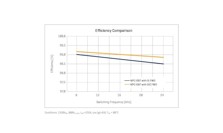
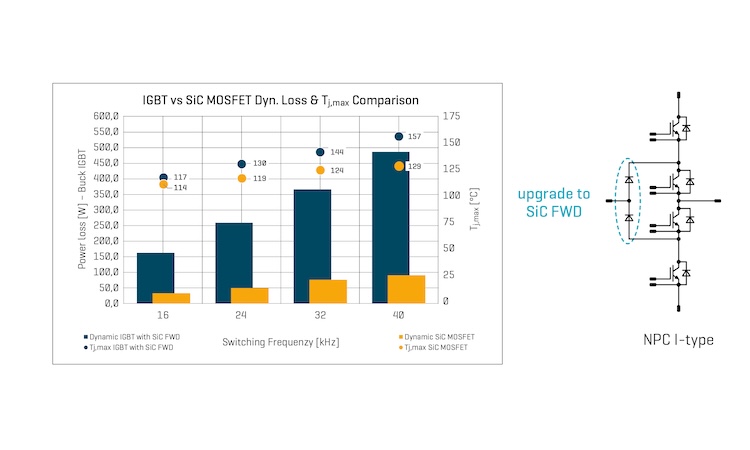
Figure 8. SiC vs Si diode in NPC I-type topology for PV inverters. Image used courtesy of Bodo’s Power Systems [PDF]
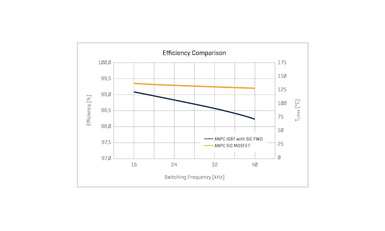
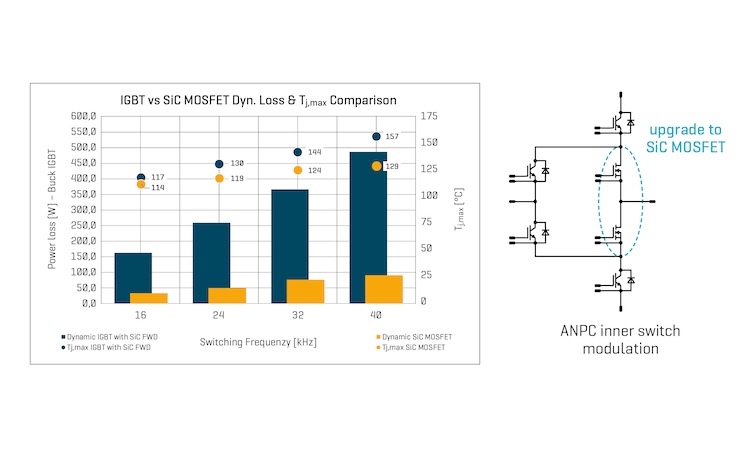
Figure 9. ANPC topology with SiC MOSFETs for ESS. Image used courtesy of Bodo’s Power Systems [PDF]
Figure 9 clearly maps out the design trade-offs engineers can make as they move from Si to SiC technology when designing for PV and ESS applications:
- Extended lifetime by lower thermal stress when switching at Si-level switching frequencies (fsw)
- Smaller, cheaper filter inductors: up to 2/3 higher switching frequencies (fsw) at comparable junction temperatures (Tj)
- Higher output power from the same housing footprint at similar junction temperatures (Tj) and switching frequency (fsw)
Summary
The adoption of SiC technology is rapidly advancing across industrial sectors due to its superior efficiency, compactness, and reliability. As these devices become more affordable and technologies continue to improve, SiC will increasingly be deployed in high-power, high-efficiency applications.
In HVAC systems, SiC enables quieter operation and improved energy efficiency, especially under partial load conditions, and helps to meet strict regulatory standards. In EV charging infrastructure, it offers high power density and fast charging up to megawatt-scale, enhancing accessibility and reducing charging times.
SiC is a key enabler in next-generation utility string inverters, sourcing more power from the same physical footprint. In ESS, it delivers efficient bidirectional performance and robustness for grid support and load balancing. In the visible future, SiC will play a key role in the transition to higher PV string voltages beyond 2 kV, helping to further reduce operating costs (€/kWh) and unlock greater system efficiency.
References
[1] “Analytical Study of SiC MOSFET Based Inverter Output dv/dt Mitigation and Loss Comparison With a Passive dv/dt Filter for High Frequency Motor Drive Applications” - Heonyiong Kim1, (Graduate Student Member, IEEE), Anup Anurag1, (Graduate Student Member, IEEE), Sayan Acharya2, (Senior Member, IEEE), and Subhashish Bhattacharya1, (Senior Member, IEEE) - 1 Department of Electrical and Computer Engineering, North Carolina State University, Raleigh, NC 27606, USA; 2ABB US Corporate Research Center, Raleigh, NC 27606, USA
[2] “General operation of Advanced Neutral Boost PFC (ANPFC)” - Vincotech´s application note, 2023.05 - https://www.vincotech.com
[3] “Highly Efficient PFC Topology Using Constant Power Control Enabling Higher Power Density and Cost Savings in Passives” - David Chilachava1, Ernö Temesi2, Marton Vazsonyi2, Gabor Ipach2 – 1 Vincotech, Germany; 2 Vincotech, Hungary. - PCIM conference 2022.
[4] “The Advantages and Operation of Flying Capacitor Booster” – Vincotech´s application note, 2024.01 - https://www.vincotech.com
[5] “Hybrid ANPC inverter with synchronous rectification” - Vincotech´s application note, 2023.11 - https://www.vincotech.com
This article originally appeared in Bodo’s Power Systems [PDF] magazine.