Facebook
 Google
 GitHub
 Linkedin
Wolfspeed Makes 300 mm Silicon Carbide Wafer Breakthrough
Single-crystal 12-inch SiC wafer production marks a significant manufacturing milestone with potential next-generation applications.
Wolfspeed has successfully produced a single-crystal 300 mm (12-inch) silicon carbide wafer. Considered an important advance in SiC substrate manufacturing, the breakthrough may have near-term implications for high-power applications like AI and HPC infrastructure.
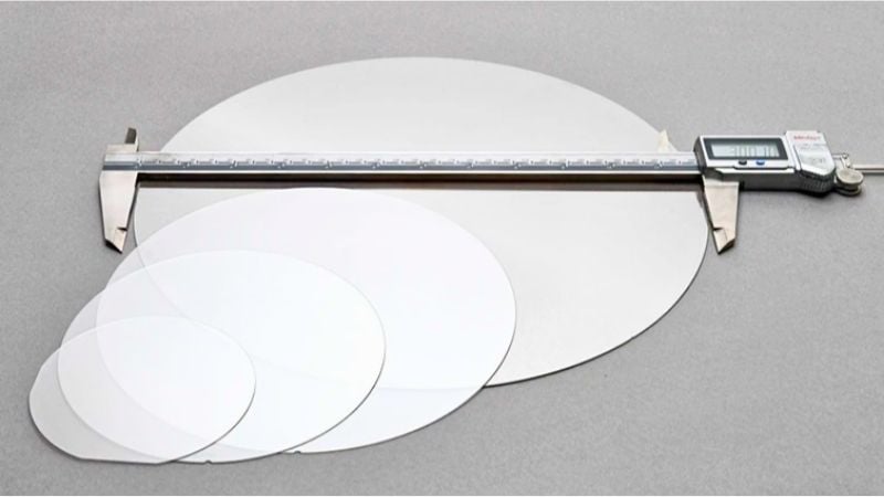
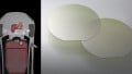
Wolfspeed’s 300 mm wafer. Image used courtesy of Wolfspeed
Wolfspeed Produces Single-Crystal 300 mm SiC Wafer
Wolfspeed reported that it has produced a single-crystal 300 mm SiC wafer as a result of sustained work in crystal growth, boule processing, and wafer processing.
From a manufacturing perspective, a move to 300 mm would change the unit economics of substrate supply and die fabrication. A larger wafer increases the theoretical number of dies per wafer and improves tool utilization when the equipment set can support the format. For example, when the silicon industry migrated to 300 mm in the early 2000s through the 2010s, cost-per-die improved dramatically at scale.
So far, for silicon carbide, the physics and process control requirements have made diameter scaling a difficult multi-variable engineering problem. Wolfspeed’s announcement implies progress toward producing single-crystal wafers at target diameters, rather than relying on bonded or composite approaches.
Wolfspeed intends its 300 mm platform to unify two substrate classes that are typically produced and optimized for different end markets. Looking to the future, the company wants to produce silicon carbide for power electronics in high volume, while also producing high-purity semi-insulating substrates for RF and optical systems. Wolfspeed converging the two could support wafer-scale integration in optical, photonic, thermal, and power domains.
The Difficulty of Scaling SiC from 200 mm to 300 mm
Scaling wafer diameter in silicon carbide is constrained first by crystal growth fundamentals.
SiC substrates begin with boule growth processes. These processes shape thermal gradients, vapor transport chemistry, and seed stability. Changes in these factors lead to variations in the substrate's dislocation density and polytype consistency.
A larger wafer presents a challenge for the boule growth processes. A larger boule diameter means the growth process must manage a larger cross-sectional area but still maintain uniform temperature and supersaturation. Here, small deviations are amplified into macroscopic defects, as well as non-uniform doping behavior and wafer-scale stress.
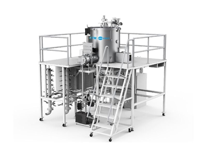
A SiC crystal growth furnace. Image used courtesy of ATW
After boule growth, the wafering and finishing stages introduce their own scaling challenges. Cutting larger-diameter SiC wafers requires tighter control of kerf loss and surface damage because SiC’s hardness calls for more aggressive mechanical processing than silicon’s. Grinding and polishing must control total thickness variation, surface roughness, and subsurface damage depth across a wider span. These parameters influence device yields because power MOSFET and diode structures depend on predictable electric-field shaping and junction termination behavior at the die edge.
Large-format wafers also stress uniformity requirements in epitaxy and device fabrication. For power devices, epitaxial layer thickness uniformity and doping concentration stability are direct levers for breakdown voltage, on-resistance, and switching behavior. As wafer diameter increases, tool uniformity and repeatability become more difficult to maintain, and the yield loss associated with edge exclusion and radial gradients becomes more economically significant.
Finally, mechanical stability limits scaling. Larger wafers face more internal stress and are more susceptible to bow and warp. In high-temperature process steps, in particular, differential thermal expansion and defect-driven stress gradients across the larger surfaces can shift wafer flatness and impact lithography overlay. Additionally, manufacturers of compound semiconductors, who are especially concerned with defect densities and wafer variability, will struggle with the extra manufacturing sensitivity.
Industrializing 300 mm SiC
A single-crystal 300 mm wafer is a long way from production maturity, but it’s a good yardstick to measure the progress of SiC substrate manufacturing. The industry must still establish repeatable processes for boule growth and wafering at 300 mm, no small tasks. However, if manufacturers are successful, they will open the door for SiC to compete with silicon and gallium nitride.