 Facebook
 Google
 GitHub
 Linkedin
Maximizing Class E Dual-frequency Resonant Boost Converter Efficiency
Discover how class E dual-frequency resonant boost converters can improve your power system efficiency. Explore advantages, disadvantages, and practical examples to help you design circuits with variable loads.
In the field of power electronics, there are a variety of DC/DC converters. Each has its mode of operation and unique features. This article will focus on the class E dual-frequency resonant boost converter, which offers many advantages over other boost converters.
Advantages of Dual-frequency Resonant Boost Converters
Compared to other boost converters, the class E dual-frequency resonant boost converter can adjust the output power if the load changes while maintaining high efficiency under all operating conditions. This is attained through its unique dual-frequency signal drive, which enables the output DC voltage to be higher than the input DC voltage with maximum efficiency.
The proposed DC/DC boost converter operating in class E with a dual-frequency signal drive can be a game-changer in power electronics. It addresses many of the challenges other boost converters face. By examining this circuit's design, operation, and performance, we can better understand its potential applications and contributions to the field of power electronics.
Boost Converter Topologies
Boost converters are widely used in power electronics to increase DC voltage. There are various topologies of boost converters, each with advantages and disadvantages.
The traditional hard-switching boost converter is the simplest and most commonly used topology. However, it suffers from high switching losses and electromagnetic interference (EMI).
On the other hand, resonant boost converters have emerged as a popular choice due to their high efficiency and reduced EMI. Several resonant boost converters include series resonant, parallel resonant, and bridgeless resonant topologies.
The series resonant boost converter has a simple circuit structure and good EI performance but suffers from high conduction losses. The parallel resonant boost converter has low conduction losses but high circulating current, leading to poor efficiency at light loads. The bridgeless resonant boost converter offers high efficiency and EMI but has a more complex circuit structure.
Class E Resonant Boost Converters for Fixed and Variable Loads
Class E converters are efficient and versatile power converters that can be used in various applications, including audio amplifiers, radio frequency (RF) transmitters, and switch-mode power supplies. The class E converter is a resonant converter that operates by switching a power transistor on and off at a high frequency, typically in tens or hundreds of kilohertz. This high switching frequency allows the converter to operate efficiently and with low losses.
One of the critical advantages of class E converters is their ability to produce unique waveforms that pass through zero before the instant of switching. This feature, known as zero-voltage-switching (ZVS), allows the converter to operate with low switching losses. In conventional switching converters, the power electronic switches interrupt the current quickly, causing high stress on the electronic components. In contrast, the ZVS feature of class E converters allows for a more gentle switching action, resulting in lower stress and power dissipation.
Another advantage of class E converters is their ability to operate over various output impedances. However, when different loads are used, a series of controls can be arranged to adjust the output signal perfectly. As the output impedance changes, the circuit's modes of operation change, as do the waveforms of the signals. Efficiency is only sometimes constant and varies, depending on the type of load applied. Nonetheless, the class E converter can still achieve high-efficiency levels.
Class E converters can also significantly increase the switching frequency compared to conventional converters, sometimes by 50 or more. This allows for high efficiencies, leading to smaller circuit sizes, reduced weight, smaller footprints, and lower final costs. The size reduction also means that the EMI aspect is dramatically reduced. The adoption of resonant circuits in converters allows for the shaping of waveforms to create zero-current-switching (ZCS) and zero-voltage-switching (ZVS) conditions. This reduces power dissipation (ideally to zero), increases switching frequency, and eliminates transient spikes, improving overall system efficiency and low EMI.
Class E converters are versatile and efficient power converters that can be used in various applications. Their ability to produce unique waveforms with zero-voltage-switching and operate over various output impedances allows for high-efficiency levels. Adopting resonant circuits in converters also allows for the shaping of waveforms to create zero-current-switching and zero-voltage-switching conditions, leading to overall system efficiency improvements and very low EMI.
Understanding Dual-Frequency Control in Boost Converters
Class E converters are a popular choice in power electronics applications due to their ability to achieve high efficiency and reduced electromagnetic interference (EMI). However, these converters are typically designed for a specific load condition and can only operate efficiently under those conditions. Any changes to the load can result in significant reductions in system efficiency.
Engineers have developed dual-frequency control for class E converters to overcome this limitation. The converter can maintain an optimal operating point regardless of the load condition by modulating the output current with two different frequencies, ensuring maximum efficiency.
In traditional switching converters, inductors are often the most critical component due to their impact on efficiency and EMI. However, the inductors can remain unchanged in a dual-frequency class E boost converter. Instead, the optimal operating point is achieved using two different switching frequencies, allowing for greater control over the waveform and reducing switching losses.
Several precautions must be taken to ensure proper operation when implementing a dual-frequency class E boost converter. The circuit must be carefully designed to minimize EMI and ensure stability. Additionally, the control circuitry must accurately switch between the two frequencies to maintain the optimal operating point, as shown in figure 1.
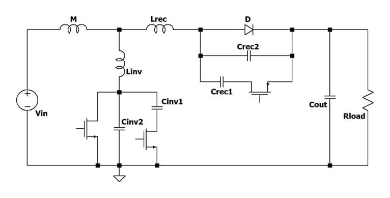
Figure 1. Schematic illustration of a dual-frequency class E boost converter. Image used courtesy of EETech
One of the advantages of the dual-frequency class E converter is that it allows the use of identical inductors without having to replace them, which can be a significant cost-saving factor. tanceInstead, the optimal operating point at both frequencies can be achieved by simply adjusting the value of the capacitors connected in parallel with the electronic switches.
It is crucial to keep the product of the output current and the switching frequency of the transistor constant to maintain maximum efficiency. This requirement is essential in both the single-frequency boost and the dual-frequency class E converter. However, the latter offers the advantage of including electronic switches that alternately connect and disconnect an additional pair of capacitors, increasing the capacitance of the circuit.
It is worth noting that when these switching devices are in conduction, they allow the additional capacitors to be connected in parallel to those already existing in the scheme, which can significantly improve the circuit's performance. However, it is of import to ensure that the product of the output current and the switching frequency remains constant to maintain maximum efficiency.
Iout1ws1= Iout2Ws2
Let us consider an example of a dual-frequency class E converter with an output current of 2 amps at a switching frequency of 10 kHz (Iout1 = 2 A and WS1=10 kHz). We want to calculate the output current at a different switching frequency, 20 kHz (WS2 = 20 kHz).
To calculate the output current at 20 kHz, use the formula Iout1ws1 = Iout2Ws2
2 A x 10 kHz = Iout2 x 20 kHz
Next, simplify the equation by dividing both sides by 20 kHz:
(2 A x 10 kHz) / 20 kHz = Iout2
This gives the following:
Iout2 = 1 A
Therefore, the output current at 20 kHz (Iout2) is 1 amp.
This calculation shows how the formula Iout1Ws1 = Iout2Ws2 calculates the output current of a dual-frequency class E converter at a different switching frequency. By manipulating the equation, engineers can design the control circuitry to maintain optimal efficiency and performance across various load conditions.
Circuit Operation
The class E dual-frequency boost converter operates at two switching frequencies, depending on the input voltage and load conditions. To achieve optimal performance at both frequencies, the circuit includes two switches in series, each with its capacitor labeled Cinv1 and Crec1. By closing these switches, the capacitances of Cinv1 and Crec1 are added to Cinv2 and Crec2, respectively, resulting in a lower switching frequency. The circuit operates at a higher frequency when these additional capacitances are disconnected.
The input and output voltages and the two maximum powers dissipated by the load must be determined at the design stage. The currents of these two branches, INV and REC, can be calculated from these values, and the inductive components can be chosen accordingly. However, this delicate process must consider the two frequencies involved.
Waveforms of the voltage between the cathode and anode of the diode V and the voltage between the drain and source of the electronic switch V (D, S) (K, A) are shown in Figure 2. The following steps should be followed to obtain good working conditions at the two chosen frequencies.
- Choose the input and output voltages.
- Determine the maximum powers at the two frequencies.
- Calculate relative currents.
- Choose the inductors and decide on the respective q-values at the two frequencies.
- Calculate the switching losses and optimize the effects by barely adjusting the issue values.
_and_V(K,_A)..jpg)
Figure 2. An oscillogram showcasing the lower frequency operation of the circuit, depicting the voltages V(D, S) and V(K, A). Image used courtesy of EETech
The components are first sized at a given frequency and then again at twice that frequency. The switching losses are recalculated, and further optimization is performed. This complex and challenging procedure requires careful consideration and attention to detail to achieve optimal efficiency at both switching frequencies.
The efficient operation of the class E boost converter requires careful consideration of parasitic resistive components in the circuit, particularly those in series with reactive components such as capacitors and inductors. These resistances can vary with frequency and are particularly relevant at higher frequencies. Although capacitive reactances are minimal, inductive reactances may attain significant values due to their lower quality factor (Q).
Two equivalent designs must be combined to enable the class E boost converter to operate at two frequencies. When the electronic switches in series with Cinv1 and Crec1 are closed, the circuit operates at a lower frequency, while opening these switches allows operation at a higher frequency.
Parasitic resistances are unavoidable at these frequencies. They can cause a small step in the V (D, S) voltage oscillogram during the device's conduction turn-on, leading to a slight increase in switching power dissipation. This step cannot be eliminated but is negligible and does not significantly affect the converter's performance. This is illustrated below in Figure 3.
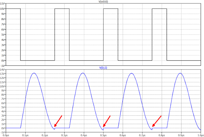
Figure 3. A small but significant step in the V(D, S) signal can be seen during transistor switching. Image used courtesy of EETech
Figure 4 presents oscillograms demonstrating the activation pulse of the electronic switch and the signals at the ends of the two semiconductor components at the base frequency and double frequency. The second mode of operation employs twice the frequency and half the current on the load, achieving results that conventional solutions at such high frequencies could not typically produce.
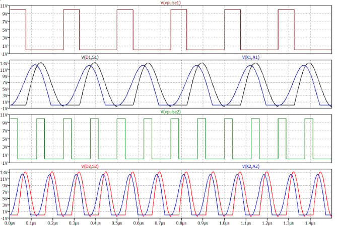
Figure 4. Graphs depicting signals at the two different operating frequencies. Image used courtesy of EETech
Takeaways of Resonant Boost Converters
The dual-frequency methodology employed in this study has significantly improved conversion efficiency, as evidenced by experimental results showing an increase of at least 6% to 7%. Thorough analysis and design have ensured that the circuits perform as intended, achieving their objectives.
To assess the system's efficiency, it is crucial to compare the voltage waveforms at the MOSFET and diode ends and analyze the currents flowing through the LINV and LREC inductors.
Class DC/DC converters are intricate and delicate but offer significant advantages in driving loads of varying nature and impedance. With extensive circuit modifications and complex arrangements, a DC/DC converter can also be implemented for three types of loads, resulting in an exponential increase in system complexity.
Featured image used courtesy of Adobe Stock


Very articulate and nice article
Written well and provides valuable insights on converters.
Hey Duke, figure 1 is not real, I can fix. You are a writer not an engineer, but that article is bogus with many errors. You should write for Trump.
Harry Dellamano