Facebook
 Google
 GitHub
 Linkedin
Improving Efficiency and Thermal Margin in a 204 W Quarter-Brick Converter Using a 150 V MOSFET
Learn how 150 V SuperQ MOSFETs boost 204 W converter efficiency greater than 0.8%, cut heat by 2 W, and lower peak temps by 31°C. They improve reliability and thermal margin in quarter-brick modules without design modifications.
This article is published by EEPower as part of an exclusive digital content partnership with Bodo’s Power Systems.
The quarter-brick DC-DC converter remains one of the most widely deployed isolated power modules in telecom infrastructure, networking equipment, industrial systems, and distributed 48V architectures. A typical implementation operating over an 18–75V input range and delivering 12V at 17A continues to serve as a workhorse intermediate bus solution in systems where footprint, thermal density, and long-term reliability are tightly constrained.
Despite the maturing of the quarter-brick format, incremental efficiency improvements on the order of 0.5–1% remain technically and economically consequential. At 200W power levels, a 1% efficiency improvement corresponds to approximately 2W reduction in dissipated heat. That reduction directly impacts thermal margin, airflow requirements, and long-term reliability. In densely populated telecom shelves or data-center racks, where dozens or hundreds of modules may be deployed, such improvements accumulate at the system level and can materially affect cooling infrastructure design and operating cost.
In recent years, increased rack-level power density in data centers and the expansion of 48V distribution architectures have intensified the need for higher efficiency within established converter footprints. Although higher-voltage distribution backbones are emerging in certain applications, the 36–75V input range remains dominant for intermediate bus conversion supplying downstream point-of-load regulators. Within this environment, designers are under pressure to improve efficiency without increasing module size or cost. As switching frequencies rise to reduce magnetics volume and improve transient response, the choice of primary-side MOSFET becomes increasingly influential.
To evaluate the impact of device selection on converter performance, testing was conducted on an off-the-shelf 204W quarterbrick power supply rated for 18–75V input, and 12V/17A output, operating at 270kHz in an active clamp forward topology (Figure 1). The default configuration utilized two 120V MOSFETs in parallel on the primary side. Comparative testing was performed by replacing the parallel pair with a single 150V MOSFET. Devices evaluated included the iS15M7R1S1C SuperQ MOSFET as well as two commercially available 150V devices representative of recent leading resistance competitors. A comparison of the evaluated devices is shown in Table 1. All testing measurements were taken at 48V input under no-airflow conditions to evaluate intrinsic electrical and thermal performance differences.
In an active clamp forward converter operating near 270kHz, primary switch losses are governed by the combined effects of conduction loss, switching overlap loss, and output capacitance discharge loss. While conduction loss has historically been the dominant loss in lower-frequency converters, at switching frequencies approaching or exceeding 250kHz, the relative contribution of switching and capacitive losses increases. Consequently, figures of merit beyond on-resistance must be considered.
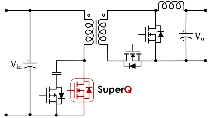
Figure 1. Active clamp forward converter schematic. Image used courtesy of Bodo’s Power Systems [PDF]
Device parameters show that the SuperQ device combines low RDS(on) with significantly reduced switching charge (QSW) and lower output capacitance energy (EOSS) compared to the evaluated alternatives. Although one competing 150V device exhibits slightly lower maximum RDS(on) under datasheet conditions, it does so at the expense of significantly higher QSW and EOSS. In a 270kHz hard-switching environment, this tradeoff materially increases switching-related dissipation.
Table 1. Devices tested in a 204W Active-Clamp Forward Converter.
|
|
SuperQ iS15M7R1S1C (x1) |
Default Configuration per FET (x2) |
Comp Gen 5 (x1) |
Comp Gen 6 (x1) |
|
BVDSS(V) |
150 V |
120 V |
150 V |
150 V |
|
RDS(ON),TYP(mΩ) |
5.4 |
9.6 |
6 |
5 |
|
RDS(ON),MAX(mΩ) |
6.4 |
11.5 |
7.4 |
5.5 |
|
EOSS(75V) (µJ) |
1 |
1.3 |
3.4 |
4.1 |
|
QSW(nC) |
4.9 |
6.8 |
14 |
15.9 |
Efficiency measurements taken at 48V input demonstrated that replacing the default dual-120V MOSFET configuration with a single 150V SuperQ device reduced total power loss by up to 2W and improved overall efficiency by more than 0.8%. For a 204W converter, this level of improvement is consistent with the calculated reductions in switching and conduction losses derived from measured QSW, EOSS, and RDS(on) values. The measured data correlated closely with calculated loss estimates, indicating that the observed performance gains are attributable to intrinsic device characteristics rather than layout or measurement artifacts.
Thermal measurements further illustrate the practical significance of these electrical differences. Under 48V input and full 17A output load with no forced airflow, the default dual-device configuration reached a peak temperature of approximately 133°C after a five-minute soak. Under identical conditions, the single 150V SuperQ MOSFET reached approximately 120.5°C.
In contrast, a representative 150V Gen6 competitor reached approximately 151.5 °C (as shown in Figure 2). The approximately 12°C reduction versus the default design and roughly 31°C reduction versus the Gen6 device are not incremental variations; they represent meaningful shifts in junction temperature. Reductions of this magnitude can substantially increase reliability margin or permit higher allowable ambient operating temperatures.
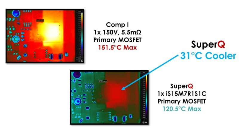
Figure 2. Thermal performance 48VIN, 17AOUT, No Air Flow, 5min soak. Image used courtesy of Bodo’s Power Systems [PDF]
The thermal data also demonstrate that reducing device count does not necessarily increase stress when intrinsic device loss is sufficiently low. The default configuration required two 120V MOSFETs in parallel to satisfy conduction and thermal requirements. The 150V SuperQ device achieved lower loss and lower peak temperature using a single device. From a system design perspective, eliminating parallel devices simplifies layout, reduces gate drive current, and mitigates parasitic imbalance concerns. It can also reduce bill-of-materials cost and improve assembly yield in high-volume production. In a cost-sensitive quarter-brick module produced at high volume, component consolidation is a meaningful advantage.
From a broader architectural perspective, 48V distribution remains dominant in telecom and networking infrastructure and is expanding within data-center environments supporting high-performance computing and AI accelerators. Although 400V and 800V backplanes are emerging, in certain applications, intermediate bus converters operating within the 36-75V range remain central to power distribution.
As system power density increases, designers continue to push switching frequency upward to reduce magnetics size and improve transient response. In this environment, minimizing switching charge and stored energy becomes as important as minimizing static resistance. Therefore, devices optimized solely for RDS(on) without simultaneous reduction in QSW and EOSS may demonstrate limited net benefit in high-frequency isolated converters.
The data presented here indicate that simultaneous optimization of RDS(on), switching charge, and output capacitance energy can produce measurable improvements in both efficiency and thermal performance within an established quarter-brick platform. In the evaluated 204W active clamp forward converter operating at 270kHz, the 150V SuperQ MOSFET delivered up to 2W lower loss, an efficiency improvement of greater than 0.8%, and up to 31°C lower peak temperature compared to representative alternatives. These results demonstrate that even in mature converter formats, careful device optimization can meaningfully extend performance limits without requiring changes to topology, magnetics design, or control architecture.
As power density requirements continue to increase across telecom and data-center applications, incremental efficiency gains at the device level remain an important lever for system optimization. The quarter-brick converter, though long-standing in form factor, continues to benefit from advances in silicon power-device architecture. By addressing conduction, switching, and capacitive losses simultaneously, it is possible to extract meaningful efficiency and thermal improvements from an established topology while preserving the cost and manufacturability advantages of silicon technology.
This article originally appeared in Bodo’s Power Systems [PDF] magazine.