 Facebook
 Google
 GitHub
 Linkedin
Reducing Electromigration in High-Voltage FACTS Semiconductors
Discover how to mitigate electromigration, a critical challenge in high-voltage semiconductors, particularly those used in flexible AC transmission systems.
Reliability is a critical concern in modern power systems, and flexible AC transmission systems (FACTS) rely heavily on functional high-voltage semiconductors. For over 100 years, semiconductor manufacturers have battled the effects of electromigration (EM), EM affects high-voltage semiconductors and eventually causes system failure. To understand how this failure occurs, we must first understand what EM is.
In electromigration, the atom of the metal conductor moves gradually over time as a result of the transfer of momentum from conducting electrons, leading to the creation of an open circuit.
In flexible AC transmission systems, components like star var compensators (SVC), unified power flow controllers (UPFC), and static synchronous compensators (STATCOM) depend on efficient high-voltage semiconductors that work to facilitate rapid current and voltage switching. EM mitigation strategies can be implemented to enhance system durability.
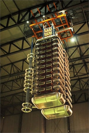
Suspended thyristor valve. Image used courtesy of ResearchGate GmbH: Neil Kirby
Electromigration-Resistant Materials Selection and Engineering
Selecting an electrical conductor material resistant to EM is essential in designing and manufacturing high-voltage semiconductor interconnects. In FACTS devices, high-voltage semiconductors spike current density up to 107 A/cm2. When copper is used for semiconductor interconnect conductivity, a high rate of EM affects reliability. Even though copper offers excellent conductivity, it is less tolerant to EM in high current densities. When considering conducting materials, two approaches can be taken to mitigate EM.

Figure 1. Electromigration is represented by the red arrow when the electrons in the wire transfer momentum, eventually resulting in contact failure. Image used courtesy of Wikimedia
One approach is using copper for the semiconductor interconnect; however, to boost its EM tolerance, the interconnects are widened or the number of parallel interconnects increased for more even current distribution. This approach reduces the current density, which affects EM and can be illustrated with the example below, where the initial cross-section (10-6 cm2) of an interconnect in a high-voltage semiconductor is doubled, and the working current is retained at 10 A.
The initial current density before widening the interconnect can be evaluated by:
\[J=\frac{I}{A}=\frac{10}{10^{-6}}=10^{7}A/cm^{2}\]
The new current density after the interconnect's cross-section is doubled:
\[J'=\frac{I}{A'}=\frac{10}{2\times10^{-6}}=5\times10^{6}A/cm^{2}\]
The reduction of current density significantly reduces electromigration in high-voltage semiconductors.
Another approach is using copper alloys and alternative conductors like tungsten and cobalt. Under high current densities, the movement of copper atoms can be controlled by increasing the EM activation energy (Ea). This energy increase can be affected by combining copper with aluminum for a more reliable interconnect. Like aluminum, magnesium can also be used as an alloying element for copper interconnects to increase EM activation energy. For instance, a 0.9 eV activation energy for pure copper can be raised to around 1.1 eV by adding 0.5 to 1% aluminum to the copper, further reducing the rate at which EM occurs. The Arrhenius-type equation describes the relationship between EM activation energy and the rate (M) at which EM occurs.
\[M=M_{0}\,exp\,exp\Big(\frac{Ea}{-kT}\Big)\]
Where the pre-exponential factor is represented by M0, K represents Boltzmann’s constant (8.617 x 10⁻⁵ eV/K), and K represents the absolute temperature of the semiconductor’s interconnects.
Thermal Management Techniques
Lower operating temperatures in high-voltage semiconductors are essential to reduce FACTS failure due to EM. These semiconductors, like gate turn-off thyristors (GTO) and insulated gate bipolar transistors (IGBT), produce heat during operations, prompting the need for effective thermal management. One such technique is a liquid cooling method, such as a dielectric, specialized coolant, and water, to uniformly dissipate heat from the semiconductor. The rate of heat transfer (Q) through a cooling medium in a cooling system can be evaluated using the formula:
\[Q=m\times Cp\times\Delta T\]
Where (m) represents the coolant’s mass flow rate given in Kg/s, (Cp) represents the coolant’s specific heat capacity, and (∆T) represents the difference in temperature between the outlet and the cooling system inlet.
During cooling system selection, the medium’s thermal resistance (Rθ ) should be lower for efficient heat dissipation. This low-temperature difference per unit power (P) in the high-voltage semiconductors significantly reduces EM. The relationship is shown below.
\[R_{\theta}=\frac{\Delta T}{P}\]
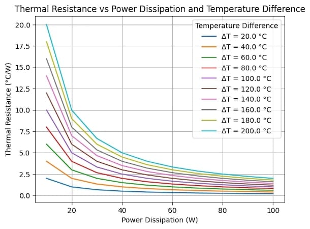
Figure 2. The relationship between power dissipation and the thermal resistance of a cooling system at varying temperatures. Image used courtesy of Bob Odhiambo
Another thermal management technique uses thermal interface materials (TIM) to improve the thermal conductivity between heat sinks and semiconductors. With thermal conductivity ranging from 10 to 20 W/m.K, graphite-based TIM offers excellent thermal conductivity, evenly dissipating heat as it conforms to any irregular surface. Phase change TIMs provide thermal conductivity alternatives as they work by changing from solid to liquid state when subjected to temperature differences.
To determine the best TIM option, consider the TIM's thermal conductivity (λ), the area of contact (A), and its thickness (d). For comparison, thermal resistance can be evaluated using the equation below, in which lower thermal resistance allows quick heat transfer, thereby reducing the effects of EM on the semiconductor's interconnects.
\[R_{\theta}=\frac{d}{\lambda\times A}\]
Electroplating and Depositing Methods
To make copper interconnects resilient to EM, electroplating is often used to deposit metallic substrates onto its surface using electric current. In this case, a metal ion solution with a higher EM tolerance is prepared, and the solution is controlled for a more even deposition. By controlling current density and deposition time, deposition uniformity can be easily achieved to significantly reduce the rate at which EM occurs in copper interconnects of semiconductors.
In addition to electroplating, physical vapor deposition (PVD) methods like evaporation and sputtering can deposit thin films of EM-resistant materials onto the surface of the interconnect material. Compared to electroplating, PVD methods offer precision in terms of deposition thickness. Sputtering occurs when the argon ions are accelerated toward an EM-resistant material to dislodge its atom. As this happens, dislodged atoms deposit onto the surface of the semiconductor's interconnect material.
On the other hand, the evaporation deposition method occurs after the EM-resistant material is heated to vapor, and as condensation takes place during cooling, deposition takes place. Another deposition approach is chemical vapor deposition (CVD), in which a solid film is formed on the interconnect's surface after a chemical reaction of volatile precursors. CVD ensures conformal coating even in intricate interconnects and is used in a range of semiconductor materials.
Mitigating Electromigration in High-Voltage Semiconductors
It is essential to ensure that high-voltage semiconductors offer stable and reliable power transfer and control and that engineers use the proper tools and techniques to mitigate the effects of electromigration in semiconductors, preventing premature failures and ensuring the reliability and durability of FACTS.


