Facebook
 Google
 GitHub
 Linkedin
Nexperia Invests $200M in WBG Semiconductors
Nexperia will expand research, development, and production capabilities for silicon carbide and gallium nitride devices at the company’s Hamburg site.
Global semiconductor company Nexperia will invest $200 million (~184 million Euros) to expand wide bandgap (WBG) semiconductor research, development, and production at its Hamburg location.
The funds will be earmarked for the next generation of efficient and power-dense silicon carbide (SiC) and gallium nitride (GaN) technologies for application in advanced energy storage, power conversion, and e-mobility applications.
Additionally, Nexperia will allocate some funding to expand its silicon (Si) wafer manufacturing capacity, producing the diodes and transistors that remain critical components in modern power system designs.
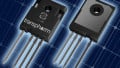
_epi_and_wafer.jpg)
Silicon carbide (SiC) epi and wafer. Image used courtesy of Nexperia
Growing Demand for Power Semiconductors
Along with its current silicon manufacturing capabilities, Nexperia will begin producing SiC and GaN devices in Germany this year, starting with high-voltage GaN D-Mode transistors and SiC diodes. Over the next few years, the company will construct a modern 200 mm production line for SiC MOSFETs and GaN HEMTs.
In addition to the WBG initiatives, the investment will automate existing infrastructure, expand silicon wafer production capacity, and add R&D laboratories to facilitate the transition of cutting-edge power semiconductor research into commercial products.
According to Achim Kempe, COO and managing director at Nexperia Germany, the new investment strengthens the company’s position as a leading supplier of efficient power semiconductors for data centers and similar applications demanding more power density and better efficiency.
Wide Bandgap Delivers More Power Density
WBG semiconductors can operate at higher frequencies and voltages than traditional silicon devices, allowing for more compact and power-dense solutions. Power density is particularly important for emerging e-mobility applications where size and weight directly impact operating time and range between charges.
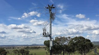
For electric vehicles, the onboard charger is a critical circuit that converts AC power from Level 1 and Level 2 chargers to high-voltage DC to replenish the vehicle’s battery pack. With very high operating frequencies, GaN FETs allow for faster switching speeds, smaller components, and a more compact, lighter solution.
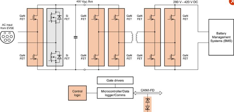
EV onboard charger circuit. Image used courtesy of Nexperia
Nexperia’s power semiconductor portfolio also includes silicon and high-voltage IGBT offerings. Each technology plays an important role dictated by the priorities and needs of individual power management applications.
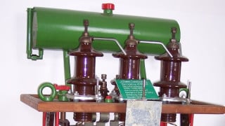
Hamburg: An Electronics History
Headquartered in the Netherlands, Nexperia has sites in Europe, North America, and Asia. The Hamburg production site was founded in 1924 as Valvo Radioröhrenfabrik, or the Valvo company. At the dawn of the radio, the company manufactured amplifier and transmitter electron tubes. The company joined the Philips group in 1927.

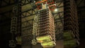
Nexperia Hamburg site. Image used courtesy of Nexperia
The Hamburg location began producing semiconductor wafers in 1953. Along with R&D, the site fab produces more than one million 6” and 8” wafers yearly, with a net yield of over one billion small-signal bipolar and discrete power devices.
Nexperia’s new investment plans were jointly announced with Hamburg’s Minister for Economic Affairs, Dr. Melanie Leonhard, on the date representing the site's 100th anniversary.