Facebook
 Google
 GitHub
 Linkedin
Breaking the Silicon Limit and Moving Beyond the SiC Ceiling
Learn how IceMOS Technology’s MEMS-based superjunction platform pushes power transistor limits, aiming to break the silicon barrier and surpass current SiC performance with advanced mSJMOS-4H-SiC architectures.
This article is published by EEPower as part of an exclusive digital content partnership with Bodo’s Power Systems.
High-voltage power conversion is at the heart of electrification, even if most people never see it. Data centers, industrial drives, medical equipment, telecom systems, renewable-energy systems, and EV charging all need power transistors that can handle high voltage, low loss, fast switching, and strong ruggedness. In this field, the question is no longer only how to improve silicon. It is how to push past the old silicon limit and now, how to challenge the current SiC limit as well. That makes device choice a direct system-level decision, not just a component choice.
IceMOS has built its story around that idea. Its MEMS Superjunction MOSFET platform, or mSJMOS, combines MEMS-style trench SOI processing with sub-micron CMOS manufacturing to create a high-voltage superjunction structure. IceMOS says the process uses bonded silicon-on-insulator substrates, deep trench etching, and oxide or polysilicon refill. This has already led to commercial silicon superjunction MOSFETs from 600 V to 730 V, and it now supports the company’s next-stage substrate roadmap.

Image used courtesy of Freepik
The value of superjunction silicon is easy to explain. By using alternating N- and P-type pillars in the drift region, the device can flatten the electric field and lower specific on-resistance without giving up blocking voltage. IceMOS stands out because it does not rely only on the usual epitaxial approach. Instead, it uses a MEMS-based process that aims to improve pillar accuracy, charge balance, and scale-up. In public material, that means low RDS(on), low gate charge, high dv/dt, strong UIS ruggedness, and high peak current capability.
That platform is already in the market. IceMOS lists Gen-1 and Gen2 products in TO-220, TO-247, DFN8x8, DFN5x6, TOLL, and DPAK packages. Examples include the 600 V ICE32S60W in TO-247 with 32 A and 0.078 Ω max RDS(on), the 650 V ICE24S65L in DFN8x8 with 24 A and 0.141 Ω max RDS(on), and the 600 V ICE47N60W in TO-247 with 47 A and 0.068 Ω max RDS(on). These parts show that IceMOS is not only talking about a roadmap. It already has real devices for high-voltage conversion.
The next part of the story is more ambitious. IceMOS is not stopping at silicon. Its roadmap points to mSJMOS-Si and mSJMOS-4HSiC structures that aim to move the blocking-voltage-versus-specific-RDS(on) curve beyond today’s best silicon and SiC devices. In the roadmap figure, Gen5 and Gen6 are shown as 4H-SiC ideas built around a symmetrical charge-balance cell design. IceMOS says the mSJMOS-4H-SiC™ GEN6 target is an estimated 0.2 mΩ-cm2, or about 10x better than current state-of-the-art SiC. This is a roadmap target, not a shipping spec, but the size of the claim is still important.
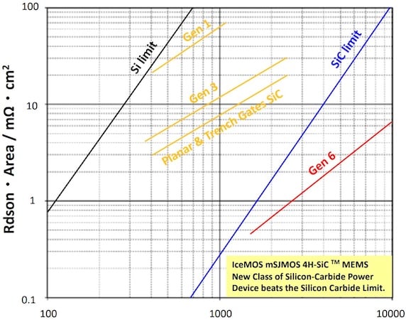
Figure 1. IceMOS mSJMOS-4H-SiC™ GEN6 roadmap: blocking voltage versus specific RDS(on) beyond the current SiC limit. Image used courtesy of Bodo’s Power Systems [PDF]
This is why the roadmap matters beyond future SiC research. Even for engineers working on present-day 600 V to 650 V systems, it shows how IceMOS sees the next step after commercial superjunction silicon. In other words, the roadmap links today’s shipping products to a longer-term device architecture strategy. It also helps explain why the company’s roadmap matters to current product decisions.
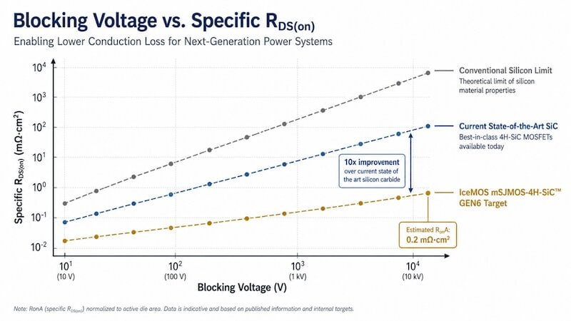
Figure 2. IceMOS mSJMOS-4H-SiC GEN6 targets and projects a 10x improvement over the state-of-the-art SiC. Image used courtesy of Bodo’s Power Systems [PDF]
The figure makes the point clear. It does not show a small step forward. It places the GEN6 target far below the current SiC limit line. That is why the message is stronger than “better SiC.” It suggests a different device structure, not just a small process tweak.
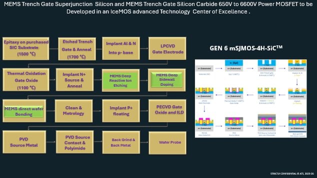
Figure 3. Advancements enabled by MEMS Processes in IceMOS GEN6 4H SiC architecture. Image used courtesy of Bodo’s Power Systems [PDF]
This is the key idea. IceMOS is trying to do to SiC what superjunction once did to silicon: break a trade-off that was once seen as fixed. In silicon, superjunction changed the link between blocking voltage and drift resistance. In the new 4H-SiC roadmap, the same charge-balance idea is being pushed into a wide-bandgap device. If it works, the result is not just a slightly better SiC MOSFET. It could be a new class of high-voltage device with much lower conduction loss.
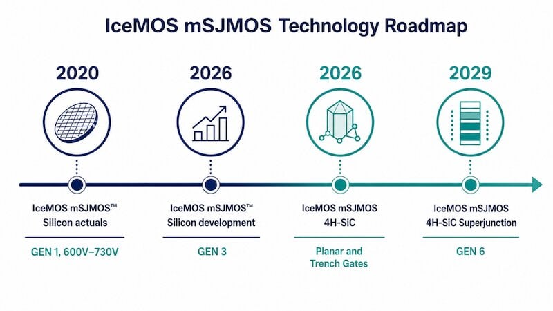
Figure 4. IceMOS mSJMOS technology roadmap from silicon actuals in 2020 to 4H-SiC superjunction GEN6 target in 2029. Image used courtesy of Bodo’s Power Systems [PDF]
This timeline works better than a patent graphic because it tells the technology story in a simple way. It starts with IceMOS mSJMOS silicon actuals in 2020, shown as Gen 1 devices from 600 V to 730 V. It then moves to silicon development in 2026, shown as Gen 3, before shifting to 4H-SiC planar and trench-gate work in 2026 and finally to 4H-SiC superjunction GEN6 in 2029. Read this way, the figure shows a real technology path from silicon superjunction products to more advanced SiC structures.
The patent story should be handled carefully, but it still matters. Public material says the patent portfolio is growing, with one 2025 company release referring to over 70 patents and later summaries referring to more than 80 granted patents. In power semiconductors, the real moat is usually not one spec number. It is the mix of process know-how, device design, manufacturing, and freedom to operate. A growing patent base supports the view that IceMOS is building a platform, not just one product line.
The overall logic is still strong. IceMOS describes a path from dielectric isolation and MEMS-enabled silicon superjunction devices to an engineered silicon-carbide drain MOSFET, with support from NASA Phase I SBIR work and later the UK Space Agency. That shows continuity. The company is not leaving silicon behind. It is carrying the same process idea into a harder SiC target.
That is also why the story should not be read as a single product claim. IceMOS is presenting a process and structure roadmap that starts with commercial silicon, moves through further silicon development, and then extends into 4H-SiC planar, trench, and superjunction concepts. This gives the company a clearer platform identity than a normal one-generation device launch.
For engineers, the short-term value is clear. IceMOS silicon superjunction devices can fit in PFC stages, auxiliary supplies, inrush protection, industrial supplies, and the slow, line-frequency leg in hybrid totem-pole PFC, where SiC or GaN is used in the fast-switching leg. In that topology, the slow leg handles the low-frequency conduction path, so cost and ruggedness matter more than extreme switching speed. That makes advanced silicon a practical choice for the slow leg. That makes it relevant not only for efficiency but also for cost, thermal design, and packaging choices.
That matters in EV charging, server power, renewable energy, and industrial drives. In these systems, even a small gain in efficiency can reduce cooling, increase power density, and lower total cost. A real step beyond today’s SiC limit would therefore be more than a lab result. It would affect the whole system. More importantly, it would mark a structural break in how engineers think about the silicon-versus-SiC roadmap. Instead of choosing between mature low-cost silicon and higher-performance SiC, designers could be looking at a new category that changes the trade-off itself. That is why the claim feels revolutionary: it is not about squeezing out one more generation of improvement, but about redrawing the device performance map.
For this readership, that is the strongest message. IceMOS is not just another superjunction silicon story, and it is not only a widebandgap story either. It is a MEMS-derived platform that first broke the silicon limit and now wants to move well beyond the current SiC ceiling. The mix of commercial silicon, a 4H-SiC roadmap, a very aggressive performance target, and a growing patent estate gives the company a clear position: the next big leap may come from rethinking the device structure itself.
This article originally appeared in Bodo’s Power Systems [PDF] magazine.