Facebook
 Google
 GitHub
 Linkedin
Enhancing the performance of traditional IGBT-module-based power assemblies with SiC modules
This article discusses how Silicon Carbide MOSFETs enable high frequency in high power conversion systems for enhanced performance of power assemblies.
In recent years, 1.2kV and 1.7kV silicon carbide (SiC) MOSFETs have become a real alternative for power converter designers who currently use IGBTs. To date, the majority of the SiC MOSFET design wins have occurred in power converters in the low watts to 20kW range, which are typically clean-sheet designs and this momentum is primarily driven by the need to improve efficiency in PV inverters and other industrial power supply applications.
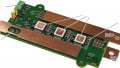
Designers are now using commercially available, high power, all-SiC power modules and drivers (see Figure 1) for both upgrading existing Si-IGBT systems and new designs especially tailored to take maximum advantage of these new SiC products to enable smaller, cooler, and all-around better-performing power conversion systems.

Figure 1: High power all-SiC power modules available in 1.2 and 1.7kV versions with their associated gate drivers are a real alternative to IGBT modules.
Si IGBT Assembly and Conversion to SiC
The material advantages of SiC over Si in power devices is well documented and requires no further review [1][2]. As such, our focus will be on the application of all-SiC modules in large power conversion systems. A commercial, off the shelf, Si-IGBT assembly based on 62mm, 400A, 1.2kV modules and including DC link capacitors, a forced air-cooled heatsink and blower, and gate drivers with protection logic and sensors was selected for SiC conversion and tested to determine performance improvements. Figure 2 depicts the IGBT assembly, which we will refer to as either an IGBT stack (before conversion) or a SiC stack (after conversion), and its critical performance specifications are shown in Figure 2, with additional details available in the manufacturer’s data sheet [3]. With a datasheet rating of 140kW (200A rms) of output power at a switching frequency (Fsw) of 3kHz, the selected 200A IGBT stack is the smallest from a family of products, and is a good representation of a generic commercial-module-based power subsystem that we are likely to find in commercial central solar inverters or motor drives.
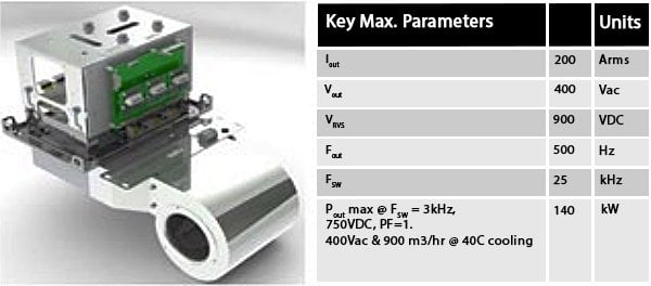
Figure 2: A commercial IGBT stack assembly and its key specifications

Figure 3: A block diagram of the IGBT stack with parts highlighted in blue is replaced or modified for the SiC stack conversion
The process involved in converting the IGBT stack to use SiC devices proved to be extremely simple due to the availability of all-SiC power modules in the same form factor with compatible gate drivers that have all of the features we see in typical IGBT module gate drivers. Figure 3 summarizes the changes. The additional DC link capacitors were only added to facilitate testing at higher output currents. The three 1200V, 400A IGBT modules were each replaced with 1200V, 300A all-SiC modules and the 6-ch gate driver board was replaced with three 2-ch gate driver boards designed for the SiC modules. One of the few mechanical changes to the SiC stack included repositioning the gate drivers from their original position, located approximately 8 inches away from the power modules, to direct mounting on the SiC modules. This modification was driven by SiC’s higher switching speeds, which necessitate that we do everything possible to minimize the effects of parasitic inductance and capacitance due to layout.
The 1200V, 300A, SiC MOSFET modules, with the built-in SiC Schottky diodes for free-wheeling, have five distinct performance advantages over the 400A IGBT modules it replaced: 1) lower switching losses, 2) lower conduction losses, 3) negligible diode switching losses, 4) higher breakdown voltage margins, and 5) immunity against cosmic radiation-induced failures or single event burnout (SEB).
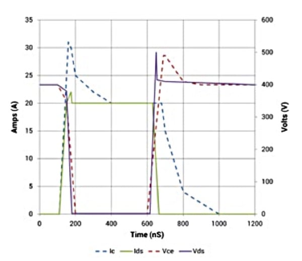
Figure 4a: MOSFET switching loss comparison
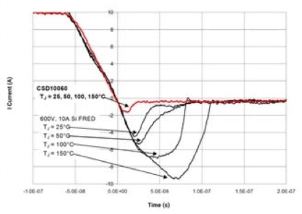
Figure 4b: MOSFET diode recovery loss comparison
It is generally a well-known fact that SiC MOSFETs have lower switching losses, as evidenced in Figure 4a, in which we compare a Si-IGBT with a fast recovery diode (FRD) in the anti-parallel position to a similarly rated SiC MOSFET with a SiC Schottky diode in the anti-parallel position of a half-bridge circuit. Note, as shown in Figure 4b, that the SiC Schottky diodes have virtually no reverse recovery charge and is constant over a temperature from 25°C to 150°C, which contributes to lower Eon in the commutating MOSFET and significantly lower diode switching losses. A lesser-known fact, however, is that the total switching losses (ET), which are the sum of turn-on and turn-off losses, in SiC MOSFETs actually remain constant or decrease with higher junction temperature (in some cases 10–25% lower), but the opposite is true for Si-IGBTs. So, at useable operating temperatures, the difference between Si-IGBT ET and SiC MOSFET ET is greater than they are at room temperature values.
In order to better understand the conduction losses, let us consider the forward characteristics of an IGBT rated for 50A to SiC MOSFETs with different current ratings. As shown in Figure 5, it is evident that an equivalent 50A SiC MOSFET will have about half the conduction losses. Plus, it is not necessary to replace a 50A IGBT with a 50A SiC device to get the same performance. The 40A SiC MOSFET and the 50A Si-IGBT both have the same conduction losses at the IGBT’s rated current. So, one may assume that both devices have the same conduction losses. However, it is important to note that the rated current of the IGBT is the DC current rating of the device for a given case temperature and does not include device switching losses. If the 50A IGBT is switching, then it will have to be de-rated to a lower current to avoid exceeding the maximum power dissipation value (PDmax) value of the part. We can see from the shape of the lines in Figure 5 that, at any value below 50A, the 40A SiC MOSFET has an advantage with regard to conduction losses due to a MOSFET’s pure Ohmic loss characteristic. Given the significant disparity if switching losses between the two devices, the SiC device will have a significantly lower current de-rating with higher switching frequencies when compared to a Si-IGBT equivalent.

Figure 5: Forward voltage vs. current comparison between IGBTs and SiC MOSFETs
Having addressed the lower switching, conduction, and diode switching losses for SiC modules, we can now discuss their immunity against high energy particle induced failures or SEB, as SiC MOSFETs are expected to be significantly less susceptible to this mode of failure. Three factors have a significant contribution towards this mode of failure: device material type, device area, and voltage stress [4].
With approximately 3x the bandgap of Si, only 33% the surface area of similarly rated Si devices, and a breakdown voltage margin 1.33 times over the maximum device voltage rating, it is easy to understand how a SiC MOSFET can minimize the effect of the three primary factors that contribute to SEB when compared to Si-IGBTs.
Enhanced Performance
After converting the IGBT stack to a SiC stack, we expected to have significantly lower power dissipation, which can result in the same output power and efficiency at much higher switching frequencies. This can reduce the size and weight of the overall system or produce more power at the same switching frequency, which can improve power density and Watts/$ or simply enable the system to operate at a lower junction temperature and higher efficiencies at the same operating conditions, effectively boosting reliability. Figure 6 shows the simulated improvement in performance, which is later verified with measured data, for output current versus switching frequency of the IGBT stack.
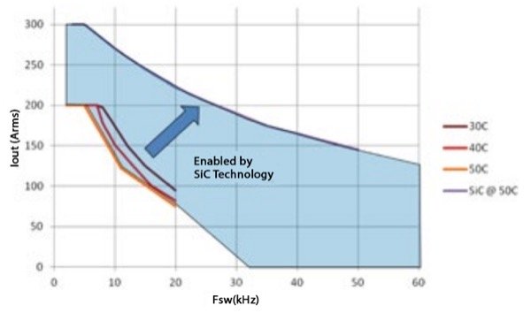
Figure 6: SiC enhanced capability, highlighted in blue, compared to the data sheet plot of the IGBT stack
To confirm the expected performance improvement, the SiC stack was tested as a 3-phase inverter, and the measured results were compared to the published datasheet values for the IGBT stack. The test was conducted using a 700VDC source with forced cooling from a 400m^3/Hr blower at an ambient temperature (TAMB) of 25°C. The output voltage was set to 480Vac rms l-l at 50Hz and connected to a balanced 3-phase resistive load bank that could be varied from 2.8 to 263kW. Initial testing was conducted at Fsw=10kHz, and then the test was repeated at Fsw=50kHz while keeping all other operating parameters constant. The results are summarized in Figure 7 and illustrate the distinct performance advantages achieved with the SiC stack.
If we consider the complete IGBT stack family, where would the converted SiC version of the stack fit in the product lineup? The answer depends on the operational switching frequency of the application. In Figure 8, we show the rated output current of the products versus Fsw. As expected, there is an inverse relationship between the output current and Fsw. However, due to the sharp de-rating of the output current for IGBT stacks, we can see that at Fsw=10kHz, the 750A rated IGBT stack, which is 3x the size of the SiC stack, has the same output current capability. Furthermore, the area highlighted in blue in Figure 8 illustrates new capabilities that are simply not economically attainable with Si-IGBTs.
Summary
High power converter designers have always had to strike a balance between performance, size, cost, and operating switching frequency (Fsw). Higher Fsw results in smaller and lighter converters, but they pay a penalty in efficiency. Typically, for high power systems (>500kW), the balancing act results in an optimal Fsw of about 3kHz. All-SiC power modules now allow design engineers to design to higher Fsw without a significant penalty on performance, tipping the scale in favor of higher frequency power conversion systems, which can result in smaller size and weight, faster response times, simplified, and more reliable power conversion systems.
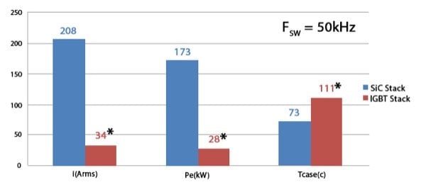
Figure 7: Output current, output power, and case temperature of the module compared before conversion (IGBT stack) and after (SiC stack) for Fsw=10kHz and Fsw=50kHz. *Denotes simulated data due to IGBT operational limitations

Figure 8: IGBT Stack product family compared with the SiC stack
About the Author
Dr. John Mookken is a director on power applications at Wolfspeed, a company that spent more than 28 years as part of Cree Inc., building the future with market-leading wide bandgap semiconductor products for the transportation, industrial, energy and communications markets.
References
- M. Bhatnagar and B. J. Baliga, “Comparison of 6H-SiC, 3C-SiC and Si for power devices,” IEEE Trans. On Electron Devices, 40 (3), pp. 645-655, March 1993.
- A Elasser, et al, “A Comparative evaluation of new silicon carbide diodes and state-of-the-art silicon diodes for power electronic applications,” IEEE IAS Annual Meeting Conference Proceedings, pp. 341-345, 1999.
- http://www.semikron.com/dl/service-support/downloads/download/ semikron-datasheet-igd-1-424-p1n4-dl-fa-08800445
- J. Dodge, “Reduce circuit zapping from cosmic radiation,” Power Electronics Technology, pp. 20-26, September 2007.
This article originally appeared in the Bodo’s Power Systems magazine.